Response Times
D-8
ET 200S Distributed I/O System
EWA-4NEB 780602402-12
Response time
The response time (t
1
to t
3
) -- that is, the time from the application of the digital
output values in internal memory until the specified value is obtained at the analog
output -- is, in the most unfavorable case, the sum of the cycle time and the settling
time. The most unfavorable case is when the analog channel is converted shortly
before the transfer of a new output value and is not converted again until after the
conversion of the other channels (cycle time).
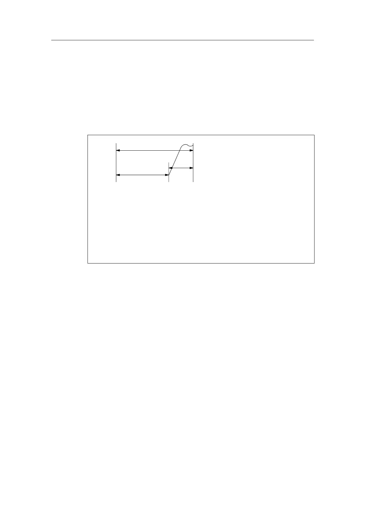
Fig. D-7 shows the response time of an analog output channel.
t
A
t
C
t
I
t
1
t
2
t
A
= response time
t
C
= cycle time according to the processing time of the module and
conversion time of the channel
t
I
= settling time
t
1
= a new digital output value is queued
t
2
= output value accepted and processed
t
3
= specified output value reached
t
3
Figure D-7 Response time of an analog output channel
D.7 Response times for a 4 IQ- SENSE electronic module
The response time of the 4 IQ-SENSE electronic module is specified as a cycle
time in the technical specifications.
D.8 Response times for process-related modules
The response times of the process-related modules are indicated as response time
or update rate in the technical specifications. See the ET 200S Process-Related
Functions manual
 Loading...