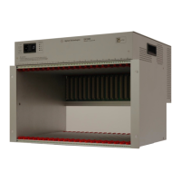
B-6 E6198B Switch/Load Unit User Manual
B Register Definitions
Fixture ID (R) Base + 3
h
The Fixture ID register contains the frame address setting of the
Frame Select Jumper (JP4). When using multiple Switch/Load
Units in your test system, Jumper JP4 provides a unique
address (0-7) for each Switch/Load Unit. Factory default (one
Switch/Load Unit) is 0.
• Default State = 255
h
• Read Only
Digital Input (R) Base + 4
h
Digital Input is a direct read-back of the logic state present on
lines Spare_DigIn[0]- Spare_DigIn[7] of the system resource
access connector J104.
DAC1 Output MSB (W) Base + 8
h
Writing to the DAC1 Output register sets the Most Significant
Bit (MSB) of the DAC1 digital input.
DAC1 Output LSB (W) Base + 9
h
Writing to the DAC1 Output register sets the Least Significant
Bit (LSB) of the DAC1 digital input.
Bits 7-0
Read
Fixture ID
Bits76543210
Read
Din
7
Din
6
Din
5
Din
4
Din
3
Din
2
Din
1
Din
0
To set the value of the DAC output, always write the MSB first, followed
by the LSB (register offset 9
h
). The output of the DAC will not update until
the LSB is written. See “DAC Scaling".
Bits76543210
Write
x xDAC1
13
DAC1
12
DAC1
11
DAC1
10
DAC1
9
DAC
8