SLM-5650B Satellite Modem
Revision 2
Introduction 1–2 MN-SLM-5650B
1.2 Functional Description
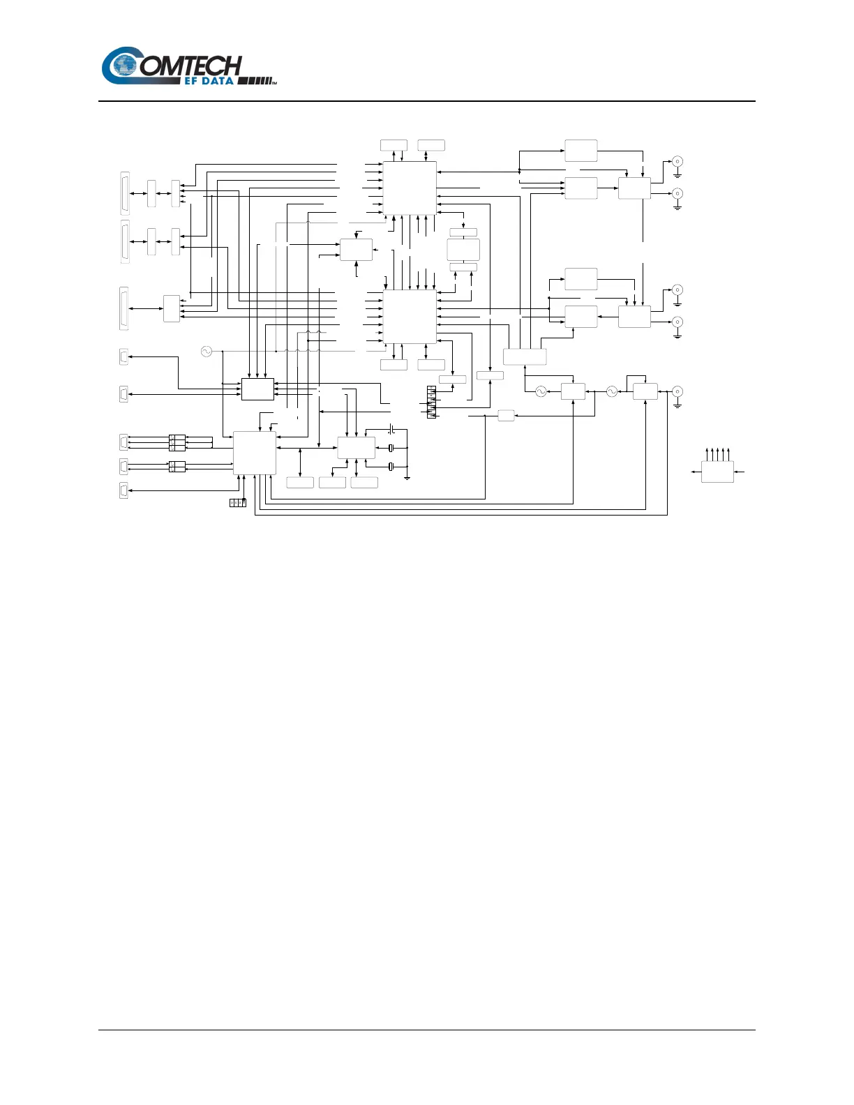
Figure 1-2. SLM-5650B Block Diagram
Figure 1-2 depicts the functional block diagram for the SLM-5650B. The modem has been
designed to accommodate a wide range of currently required features, and to support both near-
and far-term advances in software-defined radio technology as well as advances in FEC
technology. It is designed for installation in fixed or mobile Earth Terminal (ET) facilities (sites)
using Defense Satellite Communications System III (DSCS III), DSCS III/Satellite Life
Enhancement Program (SLEP), Wideband Global Satcom (WGS), and commercial satellites.
The user has the ability to:
• Add or change modular data interfaces
• Utilize an extensive array of built-in test capabilities
• Easily upgrade the modem’s operational capabilities in the field
• Easily update the modem’s firmware in the field
• Use a wide range of flexible remote control options
As shown in Figure 1-2, the modem accepts signals from a selected digital signal source and
modulates either a 70/140 MHz or L-Band Intermediate Frequency (IF) carrier with these signals.
The demodulator receives the Rx signal from either the 70/140 MHz or L-Band IF input interface,
then demodulates the IF carrier. Clock and data are recovered and output on a selected data
interface.
The Tx and Rx functions are independent with respect to coding, interleaving, overhead, and
scrambling. The modem does not allow simplex operation in the 70/140 and the L-Band IF
interfaces at the same time. The modem allows duplex operation in either one of the two IF
interfaces.
M&C – TX FPGA Lanes (1.8V)
TX FPGA
Altera 10AX066H2F34
(1.2V & 1.8
V I
/O)
2 Ch DAC
(DAC3482,
900mW)
TX RF Front
2 Ch ADC
(LTC2157-14,
650mW)
RX RF Front
R
F
L
oo
pb
a
ck
Mod
ula
tio
n I
& Q
Sy
mbo
ls
B
aseb
and
Lo
opb
ack
TX I & Q Samples (LVDS)
M&C
MVF51
NN
151
(3.3V I/O)
25MHz
EIA-530
Prim
ary Data Port
HSSI
Primary Data
Port
RJ
45
(
Modem Control)
RJ45
(Giga
Bit Interface
)
L
VDS / ECL
Tran
slator
(NB100LV
EP91)
3.3 / 1.8V
Trans
lato
r
Marvell
Ethernet
Switch
(88E6321)
EIA Pri TX (1.8V)
HSSI Pri TX (LVDS)
HSSI Pri RX (LVDS)
EIA Pri RX (1.8V)
20MHz
System Reference
250MHz VCXO
PLL
70/140MHz
TX RF Output
L-Band
TX RF Output
70/140MHz
RX RF Input
L-Band
RX RF Input
PLL
Reference Input
(1, 2, 5 or
10MHz
)
TRANSEC
(3.3V I/O)
Turbo Codec
(3.3V I/O)
DDR4
DDR4
Turbo TX
Turbo RX
3.3 / 1.8V Level
Translator
3.3 / 1.8V Level
Translator
EIA-530
Overh
ead Data Port
3.3 / 1.8
V
Translator
RX FPGA
Altera 10AX066H2F34
(1.2 & 1.8 I/O)
EIA OH TX (1.8V)
EIA OH RX (1.8V)
Alarms Remo
te Auxilia
ry
Unit Alarms
TX Alarms
RX Alarms
M&C
LCMX
02
FPGA / CPLD
(3.3V I/O)
M&C Config (1.8V)
M&C Config (3.3V)
250MHz
Clock Distributor
IP RX (RGMII)
IP TX (RGMII)
UART TX
UART RX
SD Card
Adapter
DDR 3
Front Panel
Connector
M&C Config
Hi
gh
Spe
ed T
ran
cei
ver
s
Quad 16-bit
nanoDAC
(AD5685R)
Quad 16-bit
nanoDAC
(AD5685R)
AGC
3.3 / 1.8V Level
Translator
3.3 / 1.8V Level
Translator
1.8V SPI
1.8V SPI
RX I & Q Samples (LVDS)
1.8V SPI
1.8V SPI
AGC
Power
Supply
0.
9V
1
.8
V
2
.
5V
(
f
or
D
D
R4
)
3.3V
+12V-3.3V
Option Card
Connector
IP Traffic (SerDes
)
25MHz
25MHz
1
.
2
V
(
f
o
r
D
DR
4
)
SCT DAC
SCT (LVDS & 1.8V)
SCT (L
VDS)
RXC (LVDS)
192MHz
(LVDS)
S
CT
RX
Cloc
k
10MHz Ref (3.3V)
192MHz (LVDS)
MRAM
M&C Config (3.3V)
RX Clock
DAC
24MHz
32
.
768kHz
3
V
FIPS TX (LVDS)
FIPS RX (LVDS)
RXC (LVDS & 1.8V)
M&C – RX FPGA Lanes (1.8V)
M&C – RX FPGA
Lanes (1.8V)
M&C – TX FPGA
Lanes (1.8V)
M&C
Co
nfi
g (
3.3V
)
M&C Config (MDIO)
IP Traffic (RMII)
M&C Config (1.8V)
IP Traffic (SerDes)
Differential /
Singl
e Buffe
r
Differentia
l /
Sin
gle B
uffe
r
SCT (1.8V)
RXC (1.8V)