Nano Series GigE Vision Camera Addendums • 311
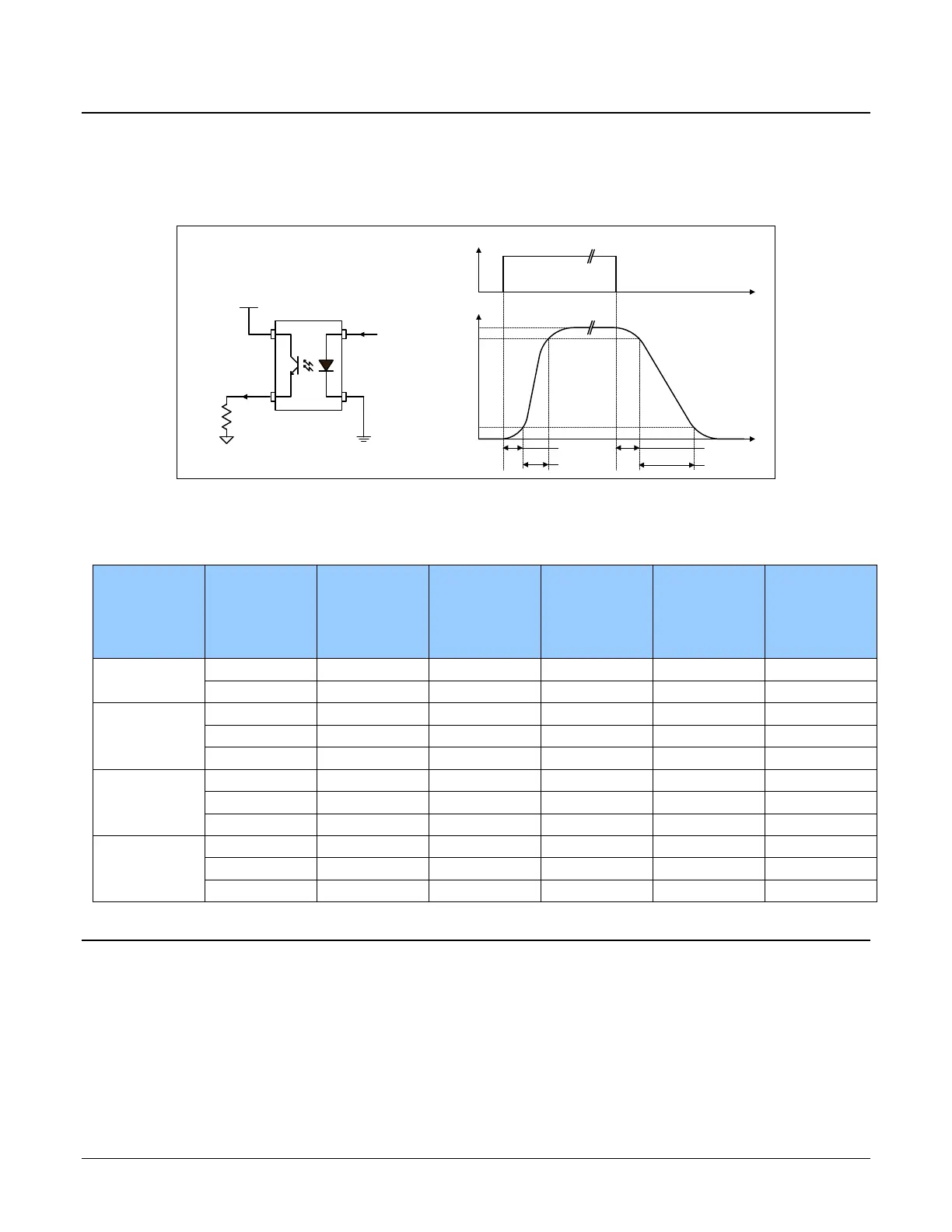
AC Characteristics of 1 Input / 3 Output Models
Optional Nano and NanoXL models with 3 outputs (see the previous section: 10-pin I/O Connector
Pinout Details (Special Order)) have output signal AC characteristics as defined in the following
table. Input characteristics remain equal to standard Nano models.
t
t
Output Control Signal
Output
100%
90%
10%
t
d1
t
rise
t
fall
t
d2
Output
Output Common Power
R
Load
Control
Signal
Opto-coupled Output:
AC Characteristics at an internal FPGA temperature of 83C
Note: All measurements subject to some rounding.
Output
Common
Power
Output
Current
R
load
Test
Teledyne
DALSA
1
(
µs)
Leading Delay
t
rise (
µs)
Rise Time
Teledyne
DALSA
2
(
µs)
Trailing Delay
t
fall (
µs)
Fall Time
3V 8 mA 250 ohm 0.5 3.4 8.5 13.4
16 mA 43 ohm 0.48 5.2 2.7 7.1
5V 8 mA 500 ohm 0.56 2.9 10.3 14.6
16 mA 170 ohm 0.52 4.9 3.3 7.4
21 mA 6.5 ohm 0.44 3.4 2.4 4.4
12V 8 mA 1.4K ohm 0.64 2.4 13.7 16.3
16 mA 625 ohm 0.61 5.4 5.2 11.1
24 mA 206 ohm 0.52 3.0 2.7 4.7
24V 8 mA 2.87K ohm 0.69 2.5 15.2 24.2
16 mA 1.35K ohm 0.69 4.7 6.2 14.4
24 mA 700 ohm 0.65 4.6 9.7 9.4
Defective Pixel Replacement (Method 4)
Important: The algorithms used exclusively with Nano firmware versions 1.00 to 1.06 are now
identified as Method 4, as described in this addendum. Nano firmware 1.07 and later implements
algorithms now identified as Method 3 and which are described in the image processing category.
The Pixel Replacement algorithm (Method 4) is based on a predefined bad pixel map (as an XML
file), either supplied by the factory (file loaded as “Factory Map”) or generated by the user (file
uploaded as “User Map 1”). The number of bad pixel entries is limited and varies dependent on the
 Loading...