1
2
3
4
5
6
7
8
© 2011 MIMAKI ENGINEERING CO.,LTD. 1.1.1 R.2.0 P.1
Maintenance Manual > Operating Principle > Basic Operation > Sequence at POWER ON
Model UJF-3042/FX Issued 2010.08.27 Revised 2011.09.30 F/W ver 1.80 / 1.00 Remark
2.0
1.1.1 Sequence at POWER ON
Sequence at turning on the power supply
The flow after turning on the power supply is as below:
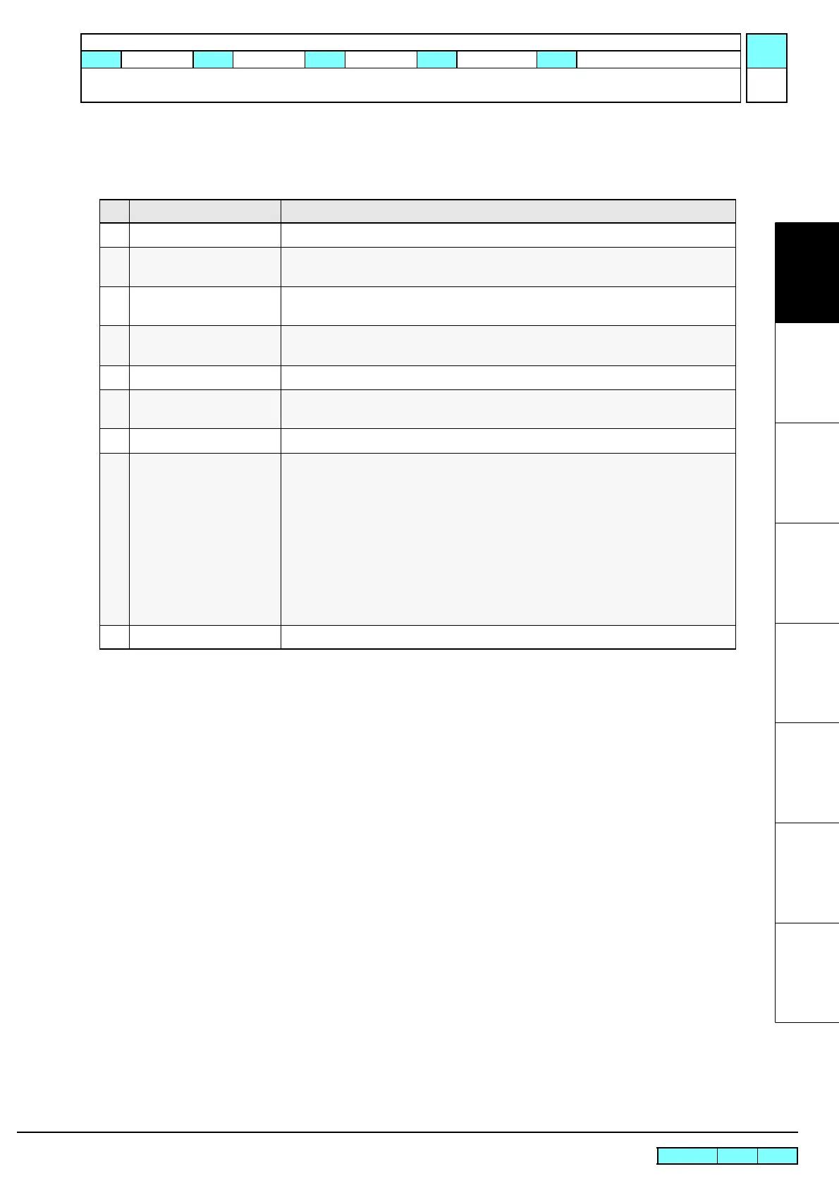
No. Item Process content
1 CPU, H/W default setting
2 S-RAM check Read/ Write check of S-RAM
This is not activated when an error has been detected.
3 F-ROM check Hash check of F-ROM
When a hash error occurs, 7-seg LED on the main PCB lights and “P” is displayed.
4 Voltage check Power Supply voltage check of Main PCB.
In the case of the abnormal detection, 7-seg LED on the main PCB lights.
5 FPGA configuration Configuration other than the slider PCB
6 SD-RAM check Read/ Write check of SD-RAM
ERROR112 is displayed and system is shut down when an error has been detected.
7 Version infomation display Turns OFF the power supply for the UV lamp (+35V) by clearing data.
8 Parameter check Parameter initialization at the initial startup after F/W version upgrade
Initializes the parameters below:
• MAINTENANCE
•SERVO
• INK2
•WAVE1
•WAVE2
•SCAN
In addition, performs check sum in the parameter area, displays ERROR202 (parameter error) and
shuts down the system.
9 Initial operation FPGA configuration of the slider PCB and origin detection operation
 Loading...