1
2
3
4
5
6
7
8
10
11
AECLKOUT
(Output from DSP)
AECLKOUT
(Input to External Device)
Control Signals
(A)
(Output from DSP)
Control Signals
(Input to External Device)
Data Signals
(B)
(Output from External Device)
Data Signals
(B)
(Input to DSP)
9
TMS320C6455
SPRS276M –MAY 2005–REVISED MARCH 2012
www.ti.com
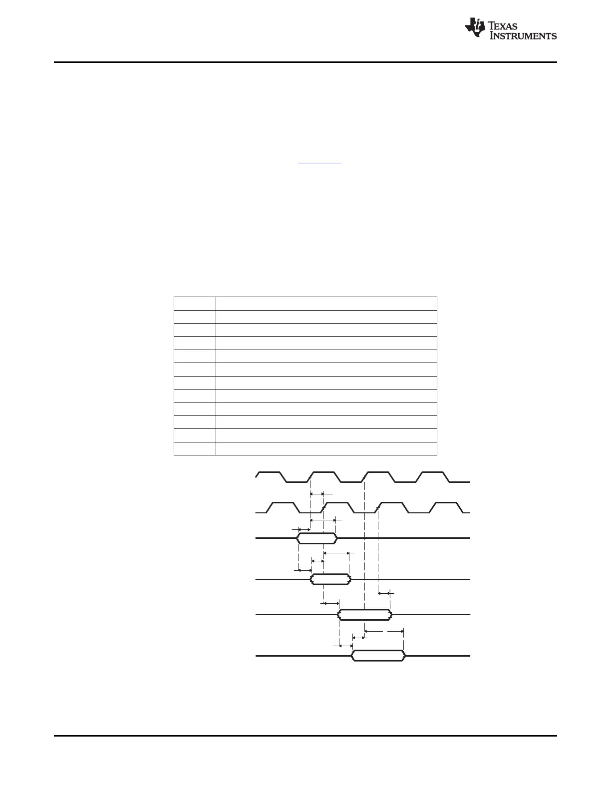
7.1.3 Timing Parameters and Board Routing Analysis
The timing parameter values specified in this data sheet do not include delays by board routings. As a
good board design practice, such delays must always be taken into account. Timing values may be
adjusted by increasing/decreasing such delays. TI recommends utilizing the available I/O buffer
information specification (IBIS) models to analyze the timing characteristics correctly. To properly use IBIS
models to attain accurate timing analysis for a given system, see the Using IBIS Models for Timing
Analysis application report (literature number SPRA839). If needed, external logic hardware such as
buffers may be used to compensate any timing differences.
For inputs, timing is most impacted by the round-trip propagation delay from the DSP to the external
device and from the external device to the DSP. This round-trip delay tends to negatively impact the input
setup time margin, but also tends to improve the input hold time margins (see Table 7-1 and Figure 7-4).
Figure 7-4 represents a general transfer between the DSP and an external device. The figure also
represents board route delays and how they are perceived by the DSP and the external device.
Table 7-1. Board-Level Timing Example
(see Figure 7-4)
NO. DESCRIPTION
1 Clock route delay
2 Minimum DSP hold time
3 Minimum DSP setup time
4 External device hold time requirement
5 External device setup time requirement
6 Control signal route delay
7 External device hold time
8 External device access time
9 DSP hold time requirement
10 DSP setup time requirement
11 Data route delay
A. Control signals include data for Writes.
B. Data signals are generated during Reads from an external device.
Figure 7-4. Board-Level Input/Output Timings
102 C64x+ Peripheral Information and Electrical Specifications Copyright © 2005–2012, Texas Instruments Incorporated
Submit Documentation Feedback
Product Folder Link(s): TMS320C6455