EasyManua.ls Logo

Texas Instruments TMS320C6455 User Manual

Texas Instruments TMS320C6455
257 pages
To Next Page IconTo Next Page
To Previous Page IconTo Previous Page
Page #114 background image
TMS320C6455
SPRS276M MAY 2005REVISED MARCH 2012
www.ti.com
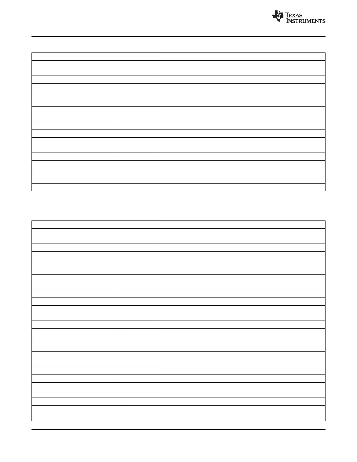
Table 7-5. EDMA3 Parameter RAM
(1)
HEX ADDRESS RANGE ACRONYM REGISTER NAME
02A0 4000 - 02A0 401F - Parameter Set 0
02A0 4020 - 02A0 403F - Parameter Set 1
02A0 4040 - 02A0 405F - Parameter Set 2
02A0 4060 - 02A0 407F - Parameter Set 3
02A0 4080 - 02A0 409F - Parameter Set 4
02A0 40A0 - 02A0 40BF - Parameter Set 5
02A0 40C0 - 02A0 40DF - Parameter Set 6
02A0 40E0 - 02A0 40FF - Parameter Set 7
02A0 4100 - 02A0 411F - Parameter Set 8
02A0 4120 - 02A0 413F - Parameter Set 9
... ...
02A0 47E0 - 02A0 47FF - Parameter Set 63
02A0 4800 - 02A0 481F - Parameter Set 64
02A0 4820 - 02A0 483F - Parameter Set 65
... ...
02A0 5FC0 - 02A0 5FDF - Parameter Set 254
02A0 5FE0 - 02A0 5FFF - Parameter Set 255
(1) The C6455 device has 256 EDMA3 parameter sets total. Each parameter set can be used as a DMA entry, a QDMA entry, or a link
entry.
Table 7-6. EDMA3 Transfer Controller 0 Registers
HEX ADDRESS RANGE ACRONYM REGISTER NAME
02A2 0000 PID Peripheral Identification Register
02A2 0004 TCCFG EDMA3TC Configuration Register
02A2 0008 - 02A2 00FC - Reserved
02A2 0100 TCSTAT EDMA3TC Channel Status Register
02A2 0104 - 02A2 011C - Reserved
02A2 0120 ERRSTAT Error Register
02A2 0124 ERREN Error Enable Register
02A2 0128 ERRCLR Error Clear Register
02A2 012C ERRDET Error Details Register
02A2 0130 ERRCMD Error Interrupt Command Register
02A2 0134 - 02A2 013C - Reserved
02A2 0140 RDRATE Read Rate Register
02A2 0144 - 02A2 023C - Reserved
02A2 0240 SAOPT Source Active Options Register
02A2 0244 SASRC Source Active Source Address Register
02A2 0248 SACNT Source Active Count Register
02A2 024C SADST Source Active Destination Address Register
02A2 0250 SABIDX Source Active Source B-Index Register
02A2 0254 SAMPPRXY Source Active Memory Protection Proxy Register
02A2 0258 SACNTRLD Source Active Count Reload Register
02A2 025C SASRCBREF Source Active Source Address B-Reference Register
02A2 0260 SADSTBREF Source Active Destination Address B-Reference Register
02A2 0264 - 02A2 027C - Reserved
02A2 0280 DFCNTRLD Destination FIFO Set Count Reload
02A2 0284 DFSRCBREF Destination FIFO Set Destination Address B Reference Register
114 C64x+ Peripheral Information and Electrical Specifications Copyright © 2005–2012, Texas Instruments Incorporated
Submit Documentation Feedback
Product Folder Link(s): TMS320C6455

Table of Contents

Other manuals for Texas Instruments TMS320C6455

Question and Answer IconNeed help?

Do you have a question about the Texas Instruments TMS320C6455 and is the answer not in the manual?

Texas Instruments TMS320C6455 Specifications

General IconGeneral
Clock Speed1.0 GHz
Core Count1
On-Chip RAMYes
Data Width32-bit
Data Bus Width64-bit
Operating Voltage1.2 V
I/O Voltage3.3 V
Instruction SetTMS320C64x+
MemoryDDR2
Package TypeBGA
External Memory InterfaceEMIF
InterfacesI2C, SPI

Summary

1 Features

2 Device Overview

2.2 CPU (DSP Core) Description

Details the C64x+ CPU core, functional units, register files, and data paths.

2.4 Boot Sequence

Explains the process of initializing the DSP's memory and registers at reset.

3 Device Configuration

3.1 Device Configuration at Device Reset

Details configuration pins (AEA, ABA, PCI_EN) for boot mode, clock source, and endianness.

5 C64x+ Megamodule

5.1 Memory Architecture

Describes the L2, L1P, and L1D memory configurations and sizes.

6 Device Operating Conditions

6.1 Absolute Maximum Ratings Over Operating Case Temperature Range (Unless Otherwise Noted)

Specifies stress ratings for voltage, temperature, and other conditions beyond which damage may occur.

6.2 Recommended Operating Conditions

Lists recommended operating ranges for supply voltages, input/output, and temperatures.

7 C64x+ Peripheral Information and Electrical Specifications

7.3 Power Supplies

Covers power supply sequencing, decoupling, and power-down operation.

7.4 Enhanced Direct Memory Access (EDMA3) Controller

Details EDMA3 features like transfer dimensions, PaRAM entries, and DMA channels.

7.6 Reset Controller

Describes different reset types (POR, Warm, Max, System, CPU) and their effects.

7.7 PLL1 and PLL1 Controller

Details PLL1 controller operation, clocks, and registers for frequency synthesis.

7.8 PLL2 and PLL2 Controller

Describes PLL2 controller operation, clocks, and registers for EMAC and DDR2 memory.

7.9 DDR2 Memory Controller

Explains DDR2 interface, device-specific information, and memory topologies.

7.10 External Memory Interface A (EMIFA)

Covers EMIFA interface capabilities for various external devices and timing.

7.11 I2C Peripheral

Describes the I2C module, its features, and device-specific information.

7.14 Ethernet MAC (EMAC)

Describes EMAC module, interface modes (MII, RMII, GMII, RGMII), and control modules.

Related product manuals