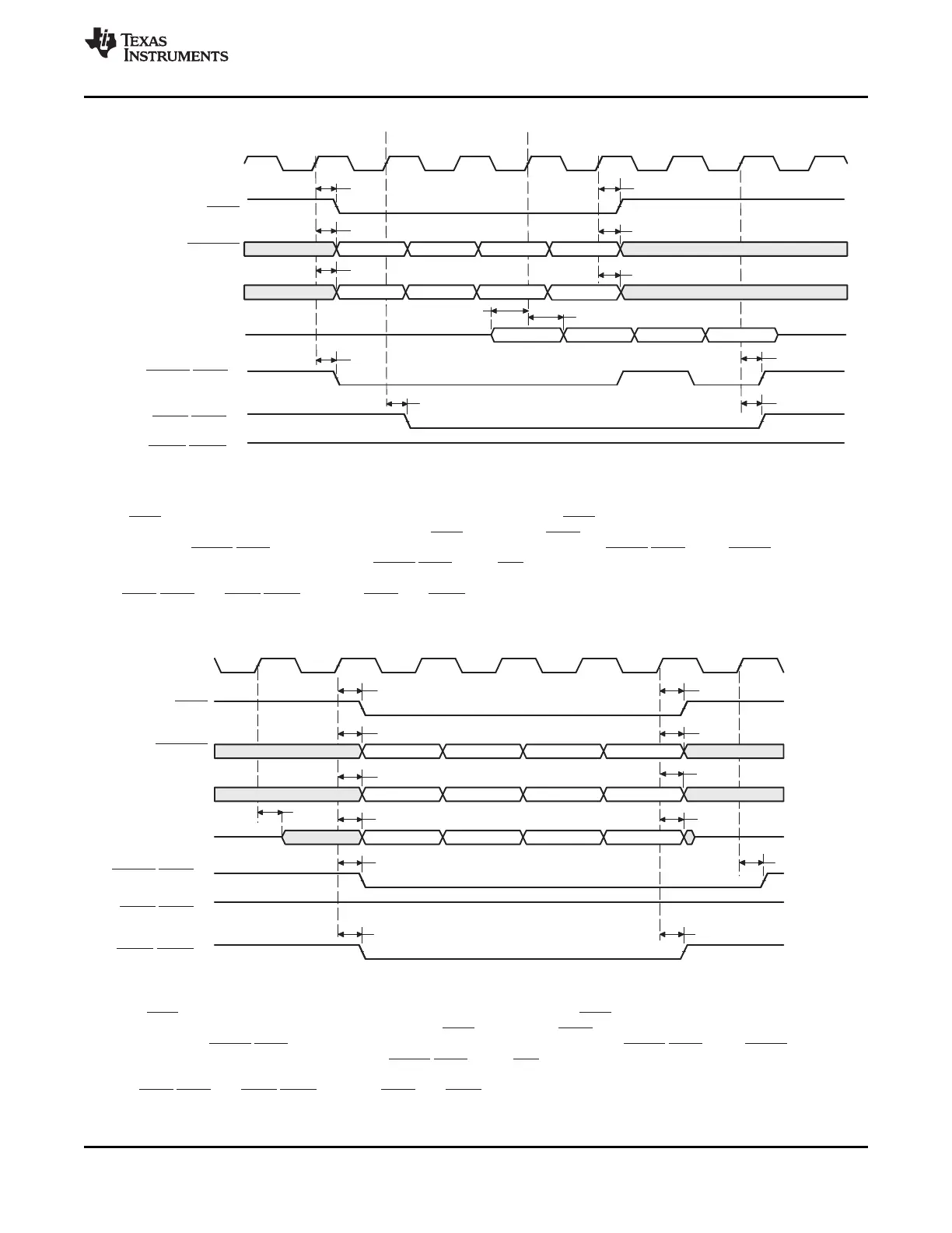
AECLKOUT
ACEx
ABE[7:0]
AEA[19:0]/ABA[1:0]
AED[63:0]
ASADS
/ASRE
(B)
AAOE
/ASOE
(B)
AAWE
/ASWE
(B)
BE1 BE2 BE3 BE4
Q1 Q2 Q3
9
1
4
5
8
9
6
7
3
1
2
BE1 BE2 BE3 BE4
EA1 EA2
EA4
8
READ latency = 2
EA3
A The following parameters are programmable via the EMIFA Chip Select n Configuration Register (CESECn):
−Read latency (R_LTNCY): 1-, 2-, or 3-cycle read latency
−Write latency (W_LTNCY): 0-, 1-, 2-, or 3-cycle write latency
−ACEx
assertion length (CE_EXT): For standard SBSRAM or ZBT SRAM interface, ACEx goes inactive after the final command has been
issued (CE_EXT = 0). For synchronous FIFO interface, ACEx
is active when ASOE is active (CE_EXT = 1).
−Function of ASADS/ASRE (R_ENABLE): For standard SBSRAM or ZBT SRAM interface, ASADS/ASRE acts as ASADS with deselect
cycles (R_ENABLE = 0). For FIFO interface, ASADS
/ASRE acts as SRE with NO deselect cycles (R_ENABLE = 1).
−In this figure R_LTNCY = 2, CE_EXT = 0, R_ENABLE = 0, and SSEL = 1.
B AAOE
/ASOE, and AAWE/ASWE operate as ASOE, and ASWE, respectively, during programmable synchronous interface accesses.
Q4
AECLKOUT
ACEx
ABE[7:0]
AEA[19:0]/ABA[1:0]
AED[63:0]
ASADS
/ASRE
(B)
AAOE
/ASOE
(B)
AAWE
/ASWE
(B)
BE1 BE2 BE3 BE4
Q1 Q2 Q3 Q4
12
11
3
1
12
10
4
2
1
8
5
8
EA1 EA2 EA3 EA4
10
A The following parameters are programmable via the EMIFA Chip Select n Configuration Register (CESECn):
− Read latency (R_LTNCY): 1-, 2-, or 3-cycle read latency
− Write latency (W_LTNCY): 0-, 1-, 2-, or 3-cycle write latency
− ACEx
assertion length (CE_EXT): For standard SBSRAM or ZBT SRAM interface, ACEx goes inactive after the final command has been
issued (CE_EXT = 0). For synchronous FIFO interface, ACEx
is active when ASOE is active (CE_EXT = 1).
− Function of ASADS/ASRE (R_ENABLE): For standard SBSRAM or ZBT SRAM interface, ASADS/ASRE acts as ASADS with deselect
cycles (R_ENABLE = 0). For FIFO interface, ASADS
/ASRE acts as SRE with NO deselect cycles (R_ENABLE = 1).
− In this figure W_LTNCY = 0, CE_EXT = 0, R_ENABLE = 0, and SSEL = 1.
B AAOE/ASOE, and AAWE/ASWE operate as ASOE, and ASWE, respectively, during programmable synchronous interface accesses.
TMS320C6455
www.ti.com
SPRS276M –MAY 2005–REVISED MARCH 2012
Figure 7-36. Programmable Synchronous Interface Read Timing for EMIFA (With Read Latency = 2)
(A)
Figure 7-37. Programmable Synchronous Interface Write Timing for EMIFA (With Write Latency = 0)
(A)
Copyright © 2005–2012, Texas Instruments Incorporated C64x+ Peripheral Information and Electrical Specifications 165
Submit Documentation Feedback
Product Folder Link(s): TMS320C6455