EasyManua.ls Logo

Texas Instruments TMS320C6455 User Manual

Texas Instruments TMS320C6455
257 pages
To Next Page IconTo Next Page
To Previous Page IconTo Previous Page
Page #4 background image
MDIO
EMAC
10/100/1000
Serial
RapidIO
DDR2
Mem Ctlr
64
C6455
HI
VCP2
I2C
16
RMGII
(D)
L2Cache
Memory
2048K
Bytes
TCP2
HPI (32/16)
(B)
DDR2 SDRAM
32
LO
Timer1
(C)
PLL2 and
PLL2
Controller
(D)
GMII
RMII
MII
Primary
Switched
Central
Resource
L2 Memory Controller
(Memory Protect/
Bandwidth Mgmt)
System
C64x+ DSP Core
Data Path B
B Register File
B31−B16
B15−B0
Instruction Fetch
Data Path A
A Register File
A31−A16
A15−A0
.L1
.S1
.M1
xx
xx
.D1 .D2
.M2
xx
xx
.S2
.L2
Internal DMA
(IDMA)
M
e
g
a
m
o
d
u
l
e
L1P Memory Controller (Memory Protect/Bandwidth Mgmt)
Instruction
Decode
16-/32-bit
Instruction Dispatch
Power Control
L1D Memory Controller (Memory Protect/Bandwidth Mgmt)
Interrupt and Exception Controller
EMIFA
HI
LO
Timer1
(C)
EDMA 3.0
Secondary
Switched Central
Resource
PLL1 and
PLL1
Controller
Device
Configuration
Logic
Boot Configuration
L1D SRAM/Cache
2-Way Set-Associative
32K Bytes Total
L1P SRAM/Cache Direct-Mapped
32K Bytes
L2 ROM
32K
Bytes
(E)
Control Registers
SPLOOP Buffer
In-Circuit Emulation
PCI66
(B)
UTOPIA
(B)
GPIO16
(B)
McBSP1
(A)
McBSP0
(A)
SBSRAM
ZBT SRAM
SRAM
ROM/FLASH
I/O Devices
A. McBSPs: Framing Chips - H.100, MVIP, SCSA, T1, E1; AC97 Devices; SPI Devices; Codecs.
B. The PCI peripheral pins are muxed with some of the HPI peripheral pins and the UTOPIA address pins.
For more detailed information, see the section.
C. Each of the TIMER peripherals (TIMER1 and TIMER0) is configurable as a 64-bit general-purpose timer, dual 32-bit general-purpose timers,
or a watchdog timer.
D. The PLL2 controller also generates clocks for the EMAC.
E. When accessing the internal ROM of the DSP, the CPU frequency must always be less than 750 MHz.
Device Configuration
TMS320C6455
SPRS276M MAY 2005REVISED MARCH 2012
www.ti.com
1.3 Functional Block Diagram
Figure 1-2 shows the functional block diagram of the C6455 device.
Figure 1-2. Functional Block Diagram
4 Features Copyright © 2005–2012, Texas Instruments Incorporated
Submit Documentation Feedback
Product Folder Link(s): TMS320C6455
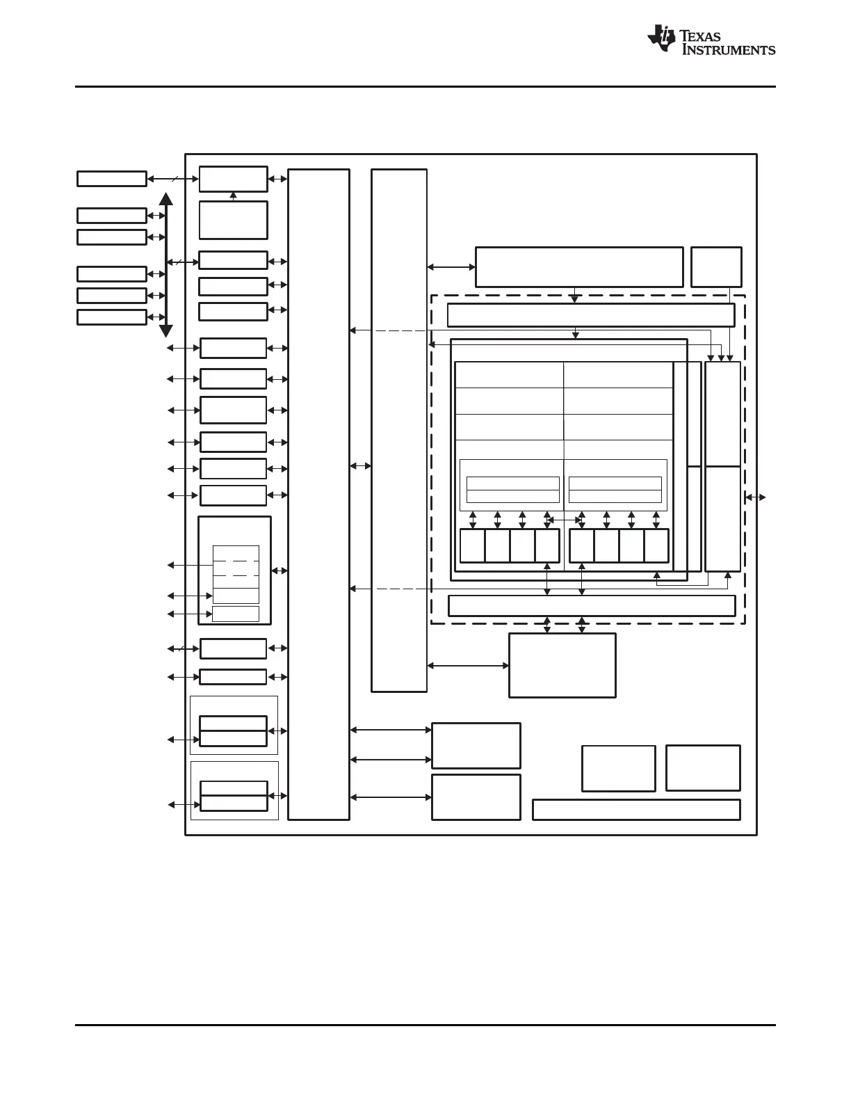
Table of Contents

Other manuals for Texas Instruments TMS320C6455

Question and Answer IconNeed help?

Do you have a question about the Texas Instruments TMS320C6455 and is the answer not in the manual?

Texas Instruments TMS320C6455 Specifications

General IconGeneral
Clock Speed1.0 GHz
Core Count1
On-Chip RAMYes
Data Width32-bit
Data Bus Width64-bit
Operating Voltage1.2 V
I/O Voltage3.3 V
Instruction SetTMS320C64x+
MemoryDDR2
Package TypeBGA
External Memory InterfaceEMIF
InterfacesI2C, SPI

Summary

1 Features

2 Device Overview

2.2 CPU (DSP Core) Description

Details the C64x+ CPU core, functional units, register files, and data paths.

2.4 Boot Sequence

Explains the process of initializing the DSP's memory and registers at reset.

3 Device Configuration

3.1 Device Configuration at Device Reset

Details configuration pins (AEA, ABA, PCI_EN) for boot mode, clock source, and endianness.

5 C64x+ Megamodule

5.1 Memory Architecture

Describes the L2, L1P, and L1D memory configurations and sizes.

6 Device Operating Conditions

6.1 Absolute Maximum Ratings Over Operating Case Temperature Range (Unless Otherwise Noted)

Specifies stress ratings for voltage, temperature, and other conditions beyond which damage may occur.

6.2 Recommended Operating Conditions

Lists recommended operating ranges for supply voltages, input/output, and temperatures.

7 C64x+ Peripheral Information and Electrical Specifications

7.3 Power Supplies

Covers power supply sequencing, decoupling, and power-down operation.

7.4 Enhanced Direct Memory Access (EDMA3) Controller

Details EDMA3 features like transfer dimensions, PaRAM entries, and DMA channels.

7.6 Reset Controller

Describes different reset types (POR, Warm, Max, System, CPU) and their effects.

7.7 PLL1 and PLL1 Controller

Details PLL1 controller operation, clocks, and registers for frequency synthesis.

7.8 PLL2 and PLL2 Controller

Describes PLL2 controller operation, clocks, and registers for EMAC and DDR2 memory.

7.9 DDR2 Memory Controller

Explains DDR2 interface, device-specific information, and memory topologies.

7.10 External Memory Interface A (EMIFA)

Covers EMIFA interface capabilities for various external devices and timing.

7.11 I2C Peripheral

Describes the I2C module, its features, and device-specific information.

7.14 Ethernet MAC (EMAC)

Describes EMAC module, interface modes (MII, RMII, GMII, RGMII), and control modules.

Related product manuals