EasyManua.ls Logo

Texas Instruments TMS320C6455 User Manual

Texas Instruments TMS320C6455
257 pages
To Next Page IconTo Next Page
To Previous Page IconTo Previous Page
Page #130 background image
CLKIN1
PCLK
RESET
RESETSTAT
SYSREFCLK (PLL1C)
Z Group
POR
SYSCLK3
SYSCLK4
SYSCLK5
AECLKOUT (Internal)
Boot and Device
Configuration Pins
Low Group
High Group
CLKIN2
Internal Reset PLL2C
SYSREFCLK (PLL2C)
SYSCLK1 (PLL2C)
SYSCLK2
5
9
7
8
Undefined
Undefined
Low
High-Z
Undefined
High
PLL2 Unlocked
PLL2 Locked
(A)
PLL2 Unlocked
Clock Valid
Undefined
Undefined
Undefined
Clock Valid
(B)
Power Supplies Ramping Power Supplies Stable
TMS320C6455
SPRS276M MAY 2005REVISED MARCH 2012
www.ti.com
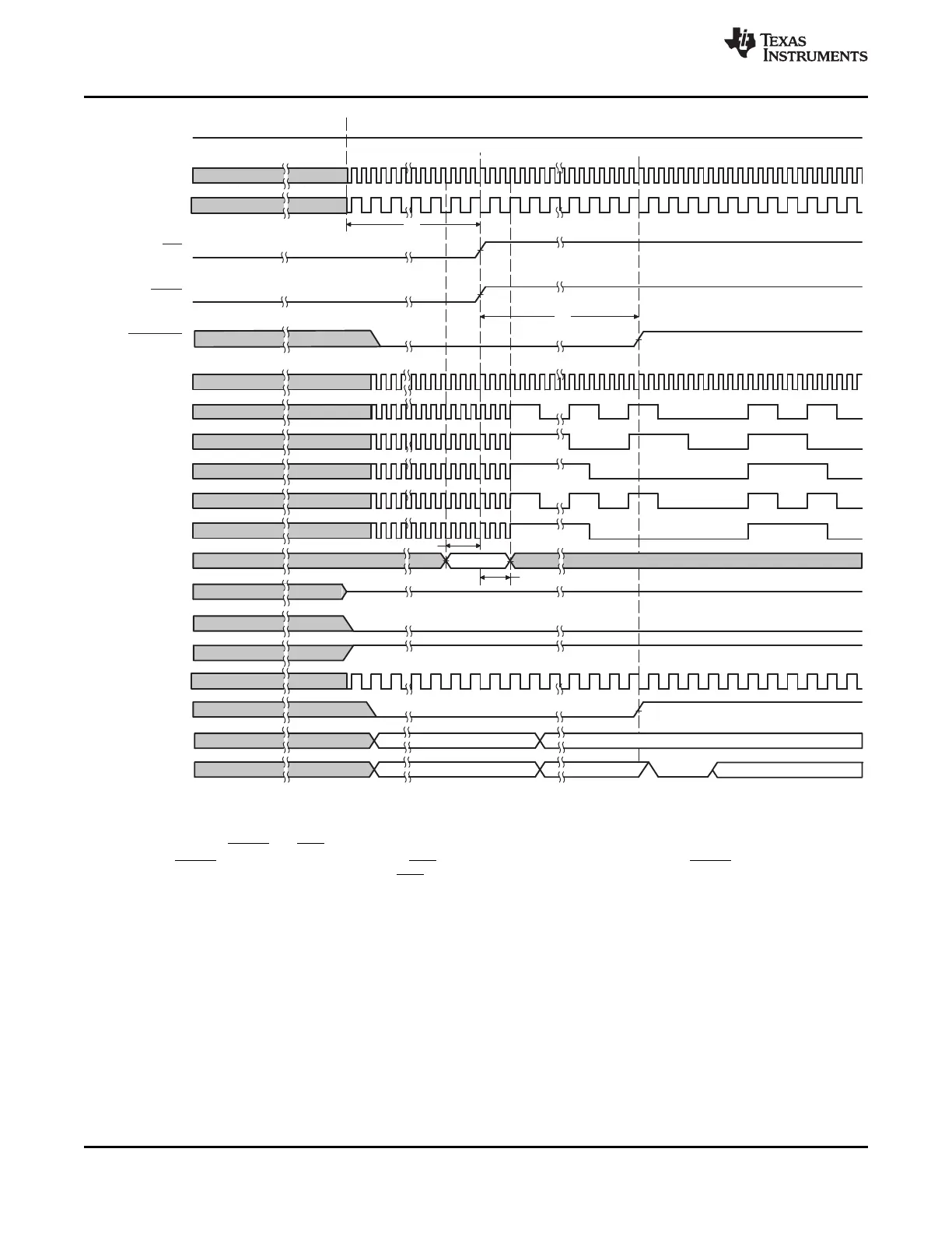
A. SYSREFCLK of the PLL2 controller runs at CLKIN2 ×10.
B. SYSCLK1 of PLL2 controller runs at SYSREFCLK/2 (default).
C. Power supplies, CLKIN1, CLKIN2 (if used), and PCLK (if used) must be stable before the start of t
w(POR)
.
D. Do not tie the RESET and POR pins together.
E. The RESET pin can be brought high after the POR pin has been brought high. In this case, the RESET pin must be
held low for a minimum of t
w(RESET)
after the POR pin has been brought high.
Figure 7-8. Power-Up Timing
130 C64x+ Peripheral Information and Electrical Specifications Copyright © 2005–2012, Texas Instruments Incorporated
Submit Documentation Feedback
Product Folder Link(s): TMS320C6455

Table of Contents

Other manuals for Texas Instruments TMS320C6455

Question and Answer IconNeed help?

Do you have a question about the Texas Instruments TMS320C6455 and is the answer not in the manual?

Texas Instruments TMS320C6455 Specifications

General IconGeneral
Clock Speed1.0 GHz
Core Count1
On-Chip RAMYes
Data Width32-bit
Data Bus Width64-bit
Operating Voltage1.2 V
I/O Voltage3.3 V
Instruction SetTMS320C64x+
MemoryDDR2
Package TypeBGA
External Memory InterfaceEMIF
InterfacesI2C, SPI

Summary

1 Features

2 Device Overview

2.2 CPU (DSP Core) Description

Details the C64x+ CPU core, functional units, register files, and data paths.

2.4 Boot Sequence

Explains the process of initializing the DSP's memory and registers at reset.

3 Device Configuration

3.1 Device Configuration at Device Reset

Details configuration pins (AEA, ABA, PCI_EN) for boot mode, clock source, and endianness.

5 C64x+ Megamodule

5.1 Memory Architecture

Describes the L2, L1P, and L1D memory configurations and sizes.

6 Device Operating Conditions

6.1 Absolute Maximum Ratings Over Operating Case Temperature Range (Unless Otherwise Noted)

Specifies stress ratings for voltage, temperature, and other conditions beyond which damage may occur.

6.2 Recommended Operating Conditions

Lists recommended operating ranges for supply voltages, input/output, and temperatures.

7 C64x+ Peripheral Information and Electrical Specifications

7.3 Power Supplies

Covers power supply sequencing, decoupling, and power-down operation.

7.4 Enhanced Direct Memory Access (EDMA3) Controller

Details EDMA3 features like transfer dimensions, PaRAM entries, and DMA channels.

7.6 Reset Controller

Describes different reset types (POR, Warm, Max, System, CPU) and their effects.

7.7 PLL1 and PLL1 Controller

Details PLL1 controller operation, clocks, and registers for frequency synthesis.

7.8 PLL2 and PLL2 Controller

Describes PLL2 controller operation, clocks, and registers for EMAC and DDR2 memory.

7.9 DDR2 Memory Controller

Explains DDR2 interface, device-specific information, and memory topologies.

7.10 External Memory Interface A (EMIFA)

Covers EMIFA interface capabilities for various external devices and timing.

7.11 I2C Peripheral

Describes the I2C module, its features, and device-specific information.

7.14 Ethernet MAC (EMAC)

Describes EMAC module, interface modes (MII, RMII, GMII, RGMII), and control modules.

Related product manuals