EasyManua.ls Logo

Texas Instruments TMS320C6455 User Manual

Texas Instruments TMS320C6455
257 pages
To Next Page IconTo Next Page
To Previous Page IconTo Previous Page
Page #91 background image
TMS320C6455
www.ti.com
SPRS276M MAY 2005REVISED MARCH 2012
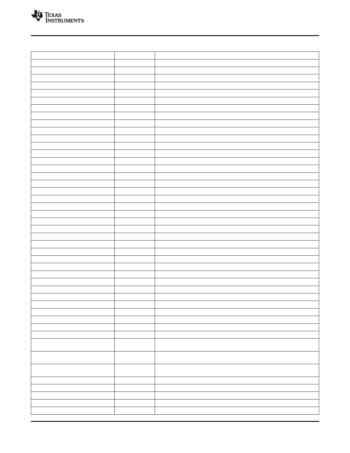
Table 5-8. Megamodule Cache Configuration Registers
HEX ADDRESS RANGE ACRONYM REGISTER NAME
0184 0000 L2CFG L2 Cache Configuration Register
0184 0004 - 0184 001F - Reserved
0184 0020 L1PCFG L1P Configuration Register
0184 0024 L1PCC L1P Cache Control Register
0184 0028 - 0184 003F - Reserved
0184 0040 L1DCFG L1D Configuration Register
0184 0044 L1DCC L1D Cache Control Register
0184 0048 - 0184 0FFF - Reserved
0184 1000 - 0184 104F - See Table 5-10, CPU Megamodule Bandwidth Management Registers
0184 1050 - 0184 3FFF - Reserved
0184 4000 L2WBAR L2 Writeback Base Address Register - for Block Writebacks
0184 4004 L2WWC L2 Writeback Word Count Register
0184 4008 - 0184 400C - Reserved
0184 4010 L2WIBAR L2 Writeback and Invalidate Base Address Register - for Block Writebacks
0184 4014 L2WIWC L2 Writeback and Invalidate word count register
0184 4018 L2IBAR L2 Invalidate Base Address Register
0184 401C L2IWC L2 Invalidate Word Count Register
0184 4020 L1PIBAR L1P Invalidate Base Address Register
0184 4024 L1PIWC L1P Invalidate Word Count Register
0184 4030 L1DWIBAR L1D Writeback and Invalidate Base Address Register
0184 4034 L1DWIWC L1D Writeback and Invalidate Word Count Register
0184 4038 - Reserved
0184 4040 L1DWBAR L1D Writeback Base Address Register - for Block Writebacks
0184 4044 L1DWWC L1D Writeback Word Count Register
0184 4048 L1DIBAR L1D Invalidate Base Address Register
0184 404C L1DIWC L1D Invalidate Word Count Register
0184 4050 - 0184 4FFF - Reserved
0184 5000 L2WB L2 Global Writeback Register
0184 5004 L2WBINV L2 Global Writeback and Invalidate Register
0184 5008 L2INV L2 Global Invalidate Register
0184 500C - 0184 5024 - Reserved
0184 5028 L1PINV L1P Global Invalidate Register
0184 502C - 0184 503C - Reserved
0184 5040 L1DWB L1D Global Writeback Register
0184 5044 L1DWBINV L1D Global Writeback and Invalidate Register
0184 5048 L1DINV L1D Global Invalidate Register
0184 504C - 0184 7FFF - Reserved
MAR0 to
0184 8000 - 0184 81FC Reserved
MAR127
MAR128 to
0184 8200 - 0184 823C Reserved
MAR143
MAR144 to
0184 8240 - 0184 827C Reserved
MAR159
0184 8280 MAR160 Controls EMIFA CE2 Range A000 0000 - A0FF FFFF
0184 8284 MAR161 Controls EMIFA CE2 Range A100 0000 - A1FF FFFF
0184 8288 MAR162 Controls EMIFA CE2 Range A200 0000 - A2FF FFFF
0184 828C MAR163 Controls EMIFA CE2 Range A300 0000 - A3FF FFFF
0184 8290 MAR164 Controls EMIFA CE2 Range A400 0000 - A4FF FFFF
Copyright © 2005–2012, Texas Instruments Incorporated C64x+ Megamodule 91
Submit Documentation Feedback
Product Folder Link(s): TMS320C6455

Table of Contents

Other manuals for Texas Instruments TMS320C6455

Question and Answer IconNeed help?

Do you have a question about the Texas Instruments TMS320C6455 and is the answer not in the manual?

Texas Instruments TMS320C6455 Specifications

General IconGeneral
Clock Speed1.0 GHz
Core Count1
On-Chip RAMYes
Data Width32-bit
Data Bus Width64-bit
Operating Voltage1.2 V
I/O Voltage3.3 V
Instruction SetTMS320C64x+
MemoryDDR2
Package TypeBGA
External Memory InterfaceEMIF
InterfacesI2C, SPI

Summary

1 Features

2 Device Overview

2.2 CPU (DSP Core) Description

Details the C64x+ CPU core, functional units, register files, and data paths.

2.4 Boot Sequence

Explains the process of initializing the DSP's memory and registers at reset.

3 Device Configuration

3.1 Device Configuration at Device Reset

Details configuration pins (AEA, ABA, PCI_EN) for boot mode, clock source, and endianness.

5 C64x+ Megamodule

5.1 Memory Architecture

Describes the L2, L1P, and L1D memory configurations and sizes.

6 Device Operating Conditions

6.1 Absolute Maximum Ratings Over Operating Case Temperature Range (Unless Otherwise Noted)

Specifies stress ratings for voltage, temperature, and other conditions beyond which damage may occur.

6.2 Recommended Operating Conditions

Lists recommended operating ranges for supply voltages, input/output, and temperatures.

7 C64x+ Peripheral Information and Electrical Specifications

7.3 Power Supplies

Covers power supply sequencing, decoupling, and power-down operation.

7.4 Enhanced Direct Memory Access (EDMA3) Controller

Details EDMA3 features like transfer dimensions, PaRAM entries, and DMA channels.

7.6 Reset Controller

Describes different reset types (POR, Warm, Max, System, CPU) and their effects.

7.7 PLL1 and PLL1 Controller

Details PLL1 controller operation, clocks, and registers for frequency synthesis.

7.8 PLL2 and PLL2 Controller

Describes PLL2 controller operation, clocks, and registers for EMAC and DDR2 memory.

7.9 DDR2 Memory Controller

Explains DDR2 interface, device-specific information, and memory topologies.

7.10 External Memory Interface A (EMIFA)

Covers EMIFA interface capabilities for various external devices and timing.

7.11 I2C Peripheral

Describes the I2C module, its features, and device-specific information.

7.14 Ethernet MAC (EMAC)

Describes EMAC module, interface modes (MII, RMII, GMII, RGMII), and control modules.

Related product manuals