TMS320C6455
www.ti.com
SPRS276M –MAY 2005–REVISED MARCH 2012
7.8.2 PLL2 Controller Memory Map
The memory map of the PLL2 controller is shown in Table 7-32. Note that only registers documented here
are accessible on the TMS320C6455 device. Other addresses in the PLL2 controller memory map should
not be modified.
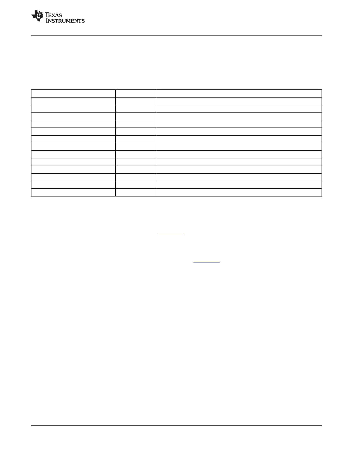
Table 7-32. PLL2 Controller Registers
HEX ADDRESS RANGE ACRONYM DESCRIPTION
029C 0000 - 029C 0114 - Reserved
029C 0118 PLLDIV1 PLL Controller Divider 1 Register
029C 011C - 029C 0134 - Reserved
029C 0138 PLLCMD PLL Controller Command Register
029C 013C PLLSTAT PLL Controller Status Register
029C 0140 ALNCTL PLL Controller Clock Align Control Register
029C 0144 DCHANGE PLLDIV Ratio Change Status Register
029C 0148 - Reserved
029C 014C - Reserved
029C 0150 SYSTAT SYSCLK Status Register
029C 0154 - 029C 0190 - Reserved
029C 0194 - 029C 01FF - Reserved
029C 0200 - 029C FFFF - Reserved
7.8.3 PLL2 Controller Register Descriptions
This section provides a description of the PLL2 controller registers. For details on the operation of the PLL
controller module, see the TMS320C645x DSP Software-Programmable Phase-Locked Loop (PLL)
Controller User's Guide (literature number SPRUE56) .
NOTE: The PLL2 controller registers can only be accessed using the CPU or the emulator.
Not all of the registers documented in the TMS320C645x DSP Software-Programmable Phase-Locked
Loop (PLL) Controller User's Guide (literature number SPRUE56) are supported on the TMS320C6455
device. Only those registers documented in this section are supported. Furthermore, only the bits within
the registers described here are supported. You should not write to any reserved memory location or
change the value of reserved bits.
Copyright © 2005–2012, Texas Instruments Incorporated C64x+ Peripheral Information and Electrical Specifications 149
Submit Documentation Feedback
Product Folder Link(s): TMS320C6455