EasyManua.ls Logo

Texas Instruments TMS320C6455 User Manual

Texas Instruments TMS320C6455
257 pages
To Next Page IconTo Next Page
To Previous Page IconTo Previous Page
Page #109 background imageLoading...
Page #109 background image
TMS320C6455
www.ti.com
SPRS276M MAY 2005REVISED MARCH 2012
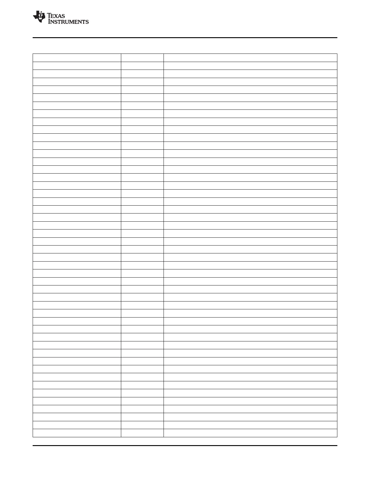
Table 7-4. EDMA3 Channel Controller Registers (continued)
HEX ADDRESS RANGE ACRONYM REGISTER NAME
02A0 01DC DCHMAP55 DMA Channel 55 Mapping Register
02A0 01E0 DCHMAP56 DMA Channel 56 Mapping Register
02A0 01E4 DCHMAP57 DMA Channel 57 Mapping Register
02A0 01E8 DCHMAP58 DMA Channel 58 Mapping Register
02A0 01EC DCHMAP59 DMA Channel 59 Mapping Register
02A0 01F0 DCHMAP60 DMA Channel 60 Mapping Register
02A0 01F4 DCHMAP61 DMA Channel 61 Mapping Register
02A0 01F8 DCHMAP62 DMA Channel 62 Mapping Register
02A0 01FC DCHMAP63 DMA Channel 63 Mapping Register
02A0 0200 QCHMAP0 QDMA Channel 0 Mapping Register
02A0 0204 QCHMAP1 QDMA Channel 1 Mapping Register
02A0 0208 QCHMAP2 QDMA Channel 2 Mapping Register
02A0 020C QCHMAP3 QDMA Channel 3 Mapping Register
02A0 0210 - 02A0 021C - Reserved
02A0 0220 - 02A0 023C - Reserved
02A0 0240 DMAQNUM0 DMA Queue Number Register 0
02A0 0244 DMAQNUM1 DMA Queue Number Register 1
02A0 0248 DMAQNUM2 DMA Queue Number Register 2
02A0 024C DMAQNUM3 DMA Queue Number Register 3
02A0 0250 DMAQNUM4 DMA Queue Number Register 4
02A0 0254 DMAQNUM5 DMA Queue Number Register 5
02A0 0258 DMAQNUM6 DMA Queue Number Register 6
02A0 025C DMAQNUM7 DMA Queue Number Register 7
02A0 0260 QDMAQNUM QDMA Queue Number Register
02A0 0264 - 02A0 0280 - Reserved
02A0 0284 QUEPRI Queue Priority Register
02A0 0288 - 02A0 02FC - Reserved
02A0 0300 EMR Event Missed Register
02A0 0304 EMRH Event MissedRegister High
02A0 0308 EMCR Event Missed Clear Register
02A0 030C EMCRH Event Missed Clear Register High
02A0 0310 QEMR QDMA Event Missed Register
02A0 0314 QEMCR QDMA Event Missed Clear Register
02A0 0318 CCERR EDMA3CC Error Register
02A0 031C CCERRCLR EDMA3CC Error Clear Register
02A0 0320 EEVAL Error Evaluate Register
02A0 0324 - 02A0 033C - Reserved
02A0 0340 DRAE0 DMA Region Access Enable Register for Region 0
02A0 0344 DRAEH0 DMA Region Access Enable Register High for Region 0
02A0 0348 DRAE1 DMA Region Access Enable Register for Region 1
02A0 034C DRAEH1 DMA Region Access Enable Register High for Region 1
02A0 0350 DRAE2 DMA Region Access Enable Register for Region 2
02A0 0354 DRAEH2 DMA Region Access Enable Register High for Region 2
02A0 0358 DRAE3 DMA Region Access Enable Register for Region 3
02A0 035C DRAEH3 DMA Region Access Enable Register High for Region 3
02A0 0360 DRAE4 DMA Region Access Enable Register for Region 4
02A0 0364 DRAEH4 DMA Region Access Enable Register High for Region 4
Copyright © 2005–2012, Texas Instruments Incorporated C64x+ Peripheral Information and Electrical Specifications 109
Submit Documentation Feedback
Product Folder Link(s): TMS320C6455

Table of Contents

Other manuals for Texas Instruments TMS320C6455

Question and Answer IconNeed help?

Do you have a question about the Texas Instruments TMS320C6455 and is the answer not in the manual?

Texas Instruments TMS320C6455 Specifications

General IconGeneral
Clock Speed1.0 GHz
Core Count1
On-Chip RAMYes
Data Width32-bit
Data Bus Width64-bit
Operating Voltage1.2 V
I/O Voltage3.3 V
Instruction SetTMS320C64x+
MemoryDDR2
Package TypeBGA
External Memory InterfaceEMIF
InterfacesI2C, SPI

Summary

1 Features

2 Device Overview

2.2 CPU (DSP Core) Description

Details the C64x+ CPU core, functional units, register files, and data paths.

2.4 Boot Sequence

Explains the process of initializing the DSP's memory and registers at reset.

3 Device Configuration

3.1 Device Configuration at Device Reset

Details configuration pins (AEA, ABA, PCI_EN) for boot mode, clock source, and endianness.

5 C64x+ Megamodule

5.1 Memory Architecture

Describes the L2, L1P, and L1D memory configurations and sizes.

6 Device Operating Conditions

6.1 Absolute Maximum Ratings Over Operating Case Temperature Range (Unless Otherwise Noted)

Specifies stress ratings for voltage, temperature, and other conditions beyond which damage may occur.

6.2 Recommended Operating Conditions

Lists recommended operating ranges for supply voltages, input/output, and temperatures.

7 C64x+ Peripheral Information and Electrical Specifications

7.3 Power Supplies

Covers power supply sequencing, decoupling, and power-down operation.

7.4 Enhanced Direct Memory Access (EDMA3) Controller

Details EDMA3 features like transfer dimensions, PaRAM entries, and DMA channels.

7.6 Reset Controller

Describes different reset types (POR, Warm, Max, System, CPU) and their effects.

7.7 PLL1 and PLL1 Controller

Details PLL1 controller operation, clocks, and registers for frequency synthesis.

7.8 PLL2 and PLL2 Controller

Describes PLL2 controller operation, clocks, and registers for EMAC and DDR2 memory.

7.9 DDR2 Memory Controller

Explains DDR2 interface, device-specific information, and memory topologies.

7.10 External Memory Interface A (EMIFA)

Covers EMIFA interface capabilities for various external devices and timing.

7.11 I2C Peripheral

Describes the I2C module, its features, and device-specific information.

7.14 Ethernet MAC (EMAC)

Describes EMAC module, interface modes (MII, RMII, GMII, RGMII), and control modules.

Related product manuals