32K bytes
32K bytes
64K bytes
128K bytes
1792K bytes
L2 memory
0080 0000h
009C 0000h
009E 0000h
009F 0000h
009F 8000h
00A0 0000h
7/8
SRAM
4-way
cache
4-way
cache
15/16
SRAM
4-way
cache
31/32
SRAM
4-way
63/64
SRAM
All
SRAM
000 001 010 011 111
Block base
address
L2 mode bits
TMS320C6455
www.ti.com
SPRS276M –MAY 2005–REVISED MARCH 2012
• Port 0 configuration:
– Memory size is 2048KB
– Starting address is 0080 0000h
– 2-cycle latency
– 4 × 128-bit bank configuration
• Port 1 configuration:
– Memory size is 32K bytes (this corresponds to the internal ROM)
– Starting address is 0010 0000h
– 1-cycle latency
– 1 × 256-bit bank configuration
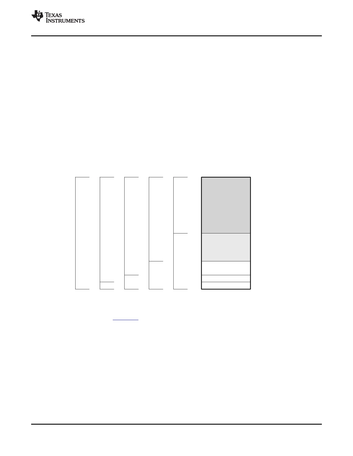
L2 memory can be configured as all SRAM or as part 4-way set-associative cache. The amount of L2
memory that is configured as cache is controlled through the L2MODE field of the L2 Configuration
Register (L2CFG) of the C64x+ Megamodule. Figure 5-4 shows the available SRAM/cache configurations
for L2. By default, L2 is configured as all SRAM after device reset.
Figure 5-4. TMS320C6455 L2 Memory Configurations
For more information on the operation L1 and L2 caches, see the TMS320C64x+ DSP Cache User's
Guide (literature number SPRU862).
All memory on the C6455 device has a unique location in the memory map (see Table 2-2).
When accessing the internal ROM of the DSP, the CPU frequency must always be less than 750 MHz.
Therefore, when using a software boot mode, care must be taken such that the CPU frequency does not
exceed 750 MHz at any point during the boot sequence. After the boot sequence has completed, the CPU
frequency can be programmed to the frequency required by the application. For more detailed information
ont he boot modes, see Section 2.4, Boot Sequence.
5.2 Memory Protection
Memory protection allows an operating system to define who or what is authorized to access L1D, L1P,
and L2 memory. To accomplish this, the L1D, L1P, and L2 memories are divided into pages. There are 16
pages of L1P (2KB each), 16 pages of L1D (2KB each), and 32 pages of L2 (64KB each). The L1D, L1P,
and L2 memory controllers in the C64x+ Megamodule are equipped with a set of registers that specify the
permissions for each memory page.
Copyright © 2005–2012, Texas Instruments Incorporated C64x+ Megamodule 85
Submit Documentation Feedback
Product Folder Link(s): TMS320C6455