4K bytes
8K bytes
16K bytes
L1P memory
00E0 0000h
00E0 4000h
00E0 6000h
00E0 7000h
00E0 8000h
direct
mapped
SRAM
1/2
dm
3/4
SRAM
SRAM
7/8
All
SRAM
000 001 010 011 100
Block base
address
L1P mode bits
cache
4K bytes
cache
direct
mapped
cache
direct
mapped
cache
4K bytes
8K bytes
16K bytes
L1D memory
00F0 0000h
00F0 4000h
00F0 6000h
00F0 7000h
00F0 8000h
2-way
SRAM
1/2
2-way
3/4
SRAM
SRAM
7/8
All
SRAM
000 001 010 011 100
Block base
address
L1D mode bits
cache
4K bytes
cache
2-way
cache
2-way
cache
TMS320C6455
SPRS276M –MAY 2005–REVISED MARCH 2012
www.ti.com
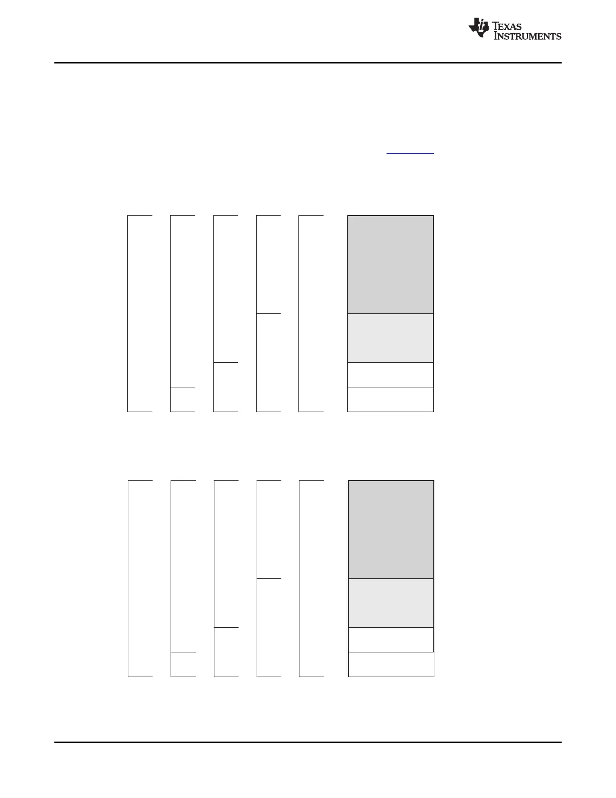
L1D is a two-way set-associative cache while L1P is a direct-mapped cache.
The L1P and L1D cache can be reconfigured via software through the L1PMODE field of the L1P
Configuration Register (L1PMODE) and the L1DMODE field of the L1D Configuration Register (L1DCFG)
of the C64x+ Megamodule. After device reset, L1P and L1D cache are configured as all cache or all
SRAM. The on-chip Bootloader changes the reset configuration for L1P and L1D. For more information,
see the TMS320C645x Bootloader User's Guide (literature number SPRUEC6) .
Figure 5-2 and Figure 5-3 show the available SRAM/cache configurations for L1P and L1D, respectively.
Figure 5-2. TMS320C6455 L1P Memory Configurations
Figure 5-3. TMS320C6455 L1D Memory Configurations
The L2 memory configuration for the C6455 device is as follows:
84 C64x+ Megamodule Copyright © 2005–2012, Texas Instruments Incorporated
Submit Documentation Feedback
Product Folder Link(s): TMS320C6455