TMS320C6455
SPRS276M –MAY 2005–REVISED MARCH 2012
www.ti.com
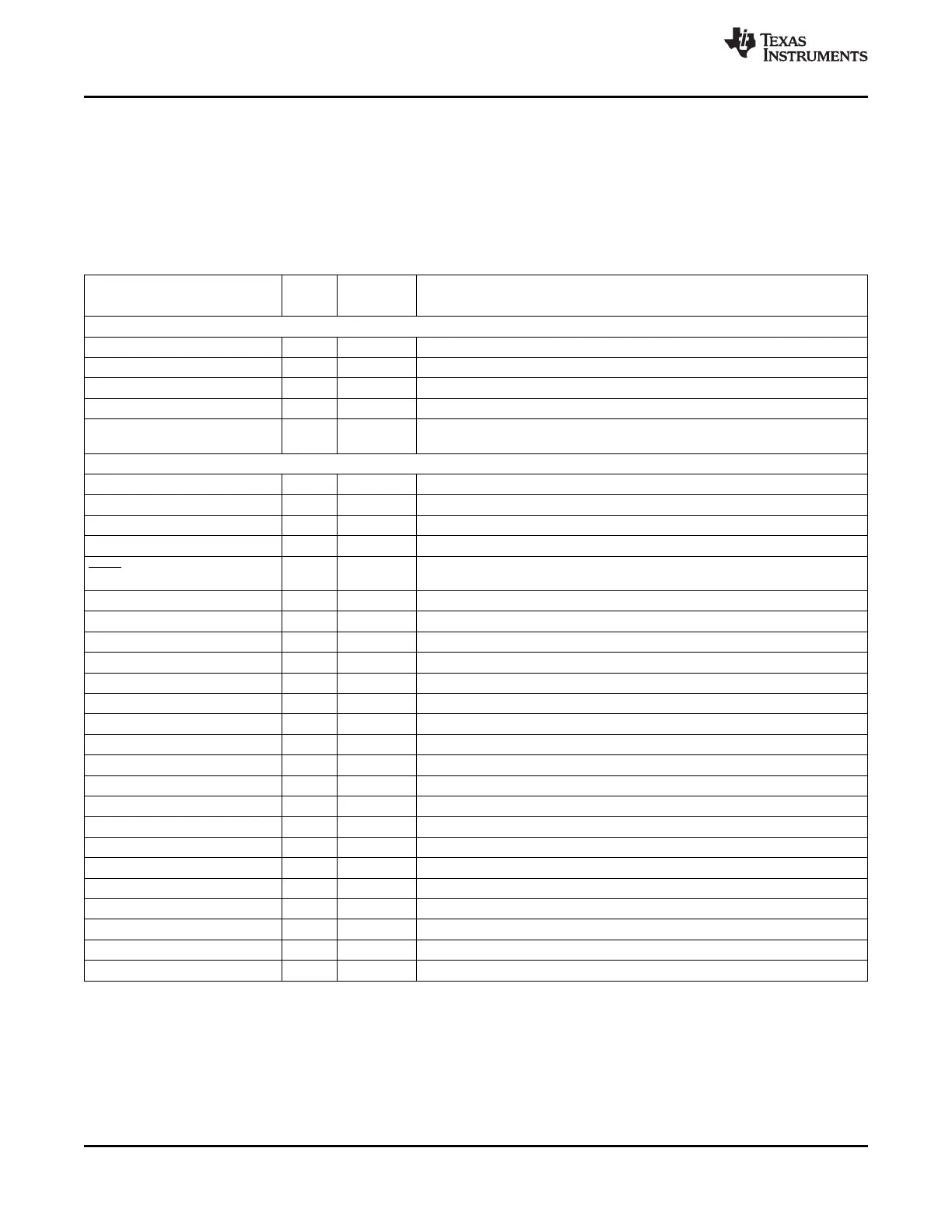
2.7 Terminal Functions
The terminal functions table (Table 2-3) identifies the external signal names, the associated pin (ball)
numbers along with the mechanical package designator, the pin type (I, O/Z, or I/O/Z), whether the pin
has any internal pullup/pulldown resistors, and a functional pin description. For more detailed information
on device configuration, peripheral selection, multiplexed/shared pins, and pullup/pulldown resistors, see
Section 3, Device Configuration.
Table 2-3. Terminal Functions
SIGNAL
TYPE
(1)
IPD/IPU
(2)
DESCRIPTION
NAME NO.
CLOCK/PLL CONFIGURATIONS
CLKIN1 N28 I IPD Clock Input for PLL1.
CLKIN2 G3 I IPD Clock Input for PLL2.
PLLV1 T29 A 1.8-V I/O supply voltage for PLL1
PLLV2 A5 A 1.8-V I/O supply voltage for PLL2
SYSCLK4 is the clock output at 1/8 of the device speed (O/Z) or this pin can be
SYSCLK4/GP[1]
(3)
AJ13 I/O/Z IPD
programmed as the GP1 pin (I/O/Z) [default].
JTAG EMULATION
TMS AJ10 I IPU JTAG test-port mode select
TDO AH8 O/Z IPU JTAG test-port data out
TDI AH9 I IPU JTAG test-port data in
TCK AJ9 I IPU JTAG test-port clock
JTAG test-port reset. For IEEE 1149.1 JTAG compatibility, see
TRST AH7 I IPD
Section 7.22.3.1.1.
EMU0
(4)
AF7 I/O/Z IPU Emulation pin 0
EMU1
(4)
AE11 I/O/Z IPU Emulation pin 1
EMU2 AG9 I/O/Z IPU Emulation pin 2
EMU3 AF10 I/O/Z IPU Emulation pin 3
EMU4 AF9 I/O/Z IPU Emulation pin 4
EMU5 AE12 I/O/Z IPU Emulation pin 5
EMU6 AG8 I/O/Z IPU Emulation pin 6
EMU7 AF12 I/O/Z IPU Emulation pin 7
EMU8 AF11 I/O/Z IPU Emulation pin 8
EMU9 AH13 I/O/Z IPU Emulation pin 9
EMU10 AD10 I/O/Z IPU Emulation pin 10
EMU11 AD12 I/O/Z IPU Emulation pin 11
EMU12 AE10 I/O/Z IPU Emulation pin 12
EMU13 AD8 I/O/Z IPU Emulation pin 13
EMU14 AF13 I/O/Z IPU Emulation pin 14
EMU15 AE9 I/O/Z IPU Emulation pin 15
EMU16 AH12 I/O/Z IPU Emulation pin 16
EMU17 AH10 I/O/Z IPU Emulation pin 17
EMU18 AE13 I/O/Z IPU Emulation pin 18
(1) I = Input, O = Output, Z = High impedance, S = Supply voltage, GND = Ground, A = Analog signal
(2) IPD = Internal pulldown, IPU = Internal pullup. For most systems, a 1-kΩ resistor can be used to oppose the IPU/IPD. For more detailed
information on pullup/pulldown resistors and situations where external pullup/pulldown resistors are required, see Section 3.7,
Pullup/Pulldown Resistors.
(3) These pins are multiplexed pins. For more details, see Section 3, Device Configuration.
(4) The C6455 DSP does not require external pulldown resistors on the EMU0 and EMU1 pins for normal or boundary-scan operation.
26 Device Overview Copyright © 2005–2012, Texas Instruments Incorporated
Submit Documentation Feedback
Product Folder Link(s): TMS320C6455