EasyManua.ls Logo

Texas Instruments TMS320C6455 User Manual

Texas Instruments TMS320C6455
257 pages
To Next Page IconTo Next Page
To Previous Page IconTo Previous Page
Page #25 background image
URADDR2/PINTA/GP[14]
Control/Status
URADDR4/PCLK/GP[2]
URDATA0/MRXD0/RMRXD0
URDATA1/MRXD1/RMRXD1
URADDR3/PREQ
/GP[15]
URADDR1/PRST
/GP[13]
URADDR0/PGNT
/GP[12]
Receive
URDATA7/MRXD7
URDATA4/MRXD4
URDATA3/MRXD3
URDATA2/MRXD2
URCLAV/MCRS/RMCRSDV
URENB
/MRXDV
URDATA5/MRXD5
URDATA6/MRXD6
URSOC/MRXER/RMRXER
URCLK/MRCLK
Clock
Control/Status
Transmit
Clock
UXADDR2/PCBE3
UXADDR4/MDCLK
UXDATA0/MTXD0/RMTXD0
UXDATA1/MTXD1/RMTXD1
UXADDR3/MDIO
UXADDR1/PIDSEL
UXADDR0/PTRDY
UXDATA7/MTXD7
UXDATA4/MTXD4
UXDATA3/MTXD3
UXDATA2/MTXD2
UXCLAV/GMTCLK
UXENB
/MTXEN/RMTXEN
UXDATA5/MTXD5
UXDATA6/MTXD6
UXSOC/MCOL/TCLKRISE
UXCLK/MTCLK/
RMREFCLK
UTOPIA (SLAVE)
(A)
A. These UTOPIA pins are muxed with the PCI or EMAC or GPIO peripherals. By default, these signals function as GPIO or EMAC peripheral
pins or have no function. For more details on these muxed pins, see the Device Configuration section of this document.
HD[15:0]/AD[15:0]
HR/W/PCBE2
HDS2/PCBE1
UXADDR4/PCBE0/GP[2]
HHWIL/PCLK
HINT/PFRAME
URADDR2/PINTA/GP[14]
Data/Address
Arbitration
32
Clock
Control
PCI Interface
(A)
HAS/PPAR
URADDR1/PRST
/GP[13]
HRDY
/PIRDY
HCNTL0/PSTOP
UXADDR0/PTRDY
UXADDR2/PCBE3
UXADDR1/PIDSEL
HCNTL1/PDEVSEL
HDS1/PSERR
Error
Command
Byte Enable
HCS/PPERR
URADDR0/PGNT/GP[12]
URADDR3/PREQ/GP[15]
HD[31:16]/AD[31:16]
A. These PCI pins are muxed with the HPI or UTOPIA or GPIO peripherals. By default, these signals function as GPIO or EMAC. For more details
on these muxed pins, see the Device Configuration section of this document.
TMS320C6455
www.ti.com
SPRS276M MAY 2005REVISED MARCH 2012
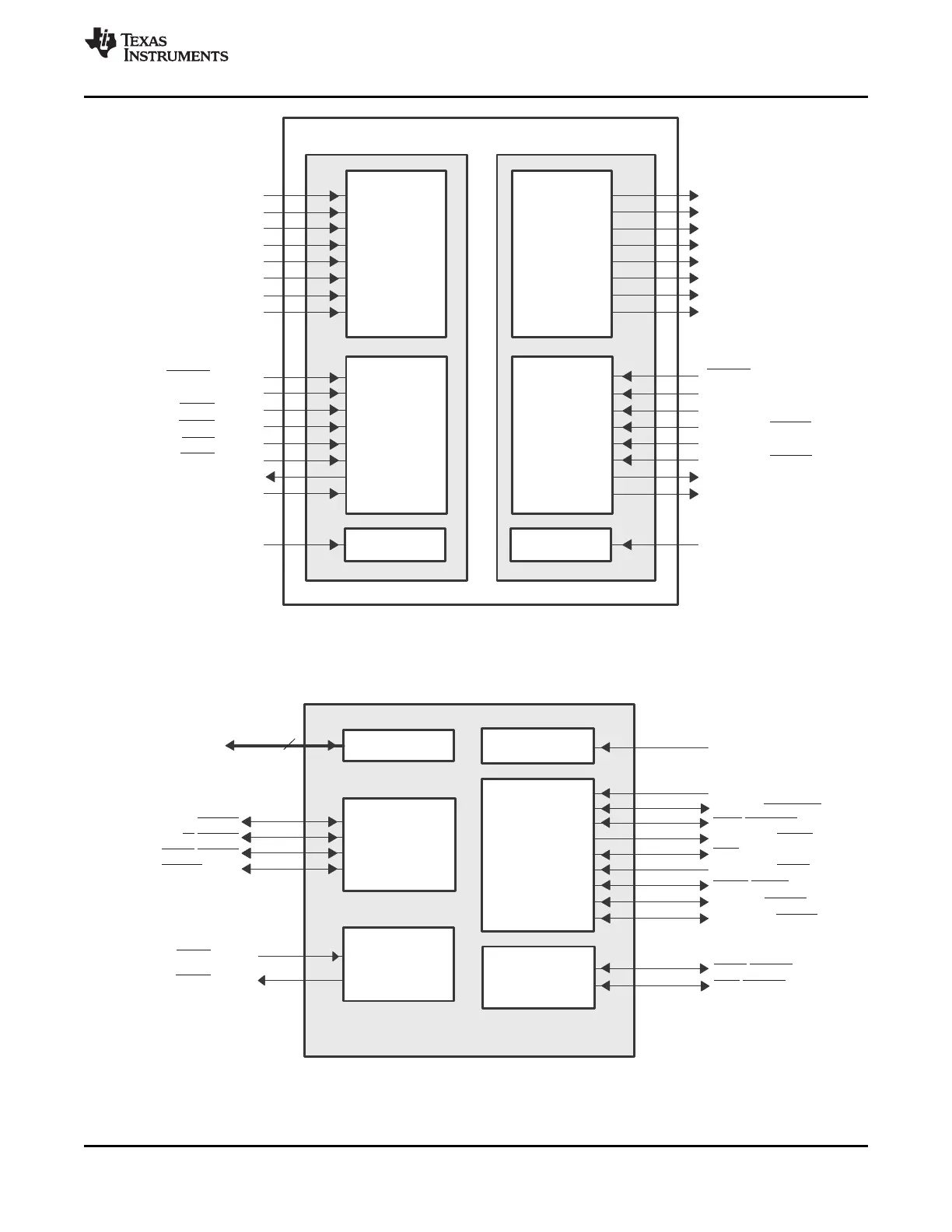
Figure 2-11. UTOPIA Peripheral Signals
Figure 2-12. PCI Peripheral Signals
Copyright © 2005–2012, Texas Instruments Incorporated Device Overview 25
Submit Documentation Feedback
Product Folder Link(s): TMS320C6455

Table of Contents

Other manuals for Texas Instruments TMS320C6455

Question and Answer IconNeed help?

Do you have a question about the Texas Instruments TMS320C6455 and is the answer not in the manual?

Texas Instruments TMS320C6455 Specifications

General IconGeneral
Clock Speed1.0 GHz
Core Count1
On-Chip RAMYes
Data Width32-bit
Data Bus Width64-bit
Operating Voltage1.2 V
I/O Voltage3.3 V
Instruction SetTMS320C64x+
MemoryDDR2
Package TypeBGA
External Memory InterfaceEMIF
InterfacesI2C, SPI

Summary

1 Features

2 Device Overview

2.2 CPU (DSP Core) Description

Details the C64x+ CPU core, functional units, register files, and data paths.

2.4 Boot Sequence

Explains the process of initializing the DSP's memory and registers at reset.

3 Device Configuration

3.1 Device Configuration at Device Reset

Details configuration pins (AEA, ABA, PCI_EN) for boot mode, clock source, and endianness.

5 C64x+ Megamodule

5.1 Memory Architecture

Describes the L2, L1P, and L1D memory configurations and sizes.

6 Device Operating Conditions

6.1 Absolute Maximum Ratings Over Operating Case Temperature Range (Unless Otherwise Noted)

Specifies stress ratings for voltage, temperature, and other conditions beyond which damage may occur.

6.2 Recommended Operating Conditions

Lists recommended operating ranges for supply voltages, input/output, and temperatures.

7 C64x+ Peripheral Information and Electrical Specifications

7.3 Power Supplies

Covers power supply sequencing, decoupling, and power-down operation.

7.4 Enhanced Direct Memory Access (EDMA3) Controller

Details EDMA3 features like transfer dimensions, PaRAM entries, and DMA channels.

7.6 Reset Controller

Describes different reset types (POR, Warm, Max, System, CPU) and their effects.

7.7 PLL1 and PLL1 Controller

Details PLL1 controller operation, clocks, and registers for frequency synthesis.

7.8 PLL2 and PLL2 Controller

Describes PLL2 controller operation, clocks, and registers for EMAC and DDR2 memory.

7.9 DDR2 Memory Controller

Explains DDR2 interface, device-specific information, and memory topologies.

7.10 External Memory Interface A (EMIFA)

Covers EMIFA interface capabilities for various external devices and timing.

7.11 I2C Peripheral

Describes the I2C module, its features, and device-specific information.

7.14 Ethernet MAC (EMAC)

Describes EMAC module, interface modes (MII, RMII, GMII, RGMII), and control modules.

Related product manuals