1
0
0
DIVIDER D4
CLKIN1
(B)
PLLEN (PLLCTL.[0])
SYSCLK2
SYSCLK3
AECLKIN (External EMIF Clock Input)
EMIFA
DIVIDER PREDIV
DIVIDER D2
(A)
DIVIDER D3
(A)
AECLKOUT
PLLV1
C2
C1
EMI Filter
+1.8 V
560 pF 0.1 µF
SYSCLK5
(Emulation and Trace)
SYSREFCLK
(C64x+ MegaModule)
AECLKINSEL
(AEA[15] pin)
DIVIDER D5
PLL1 Controller
(EMIF Input Clock)
TMS320C6455 DSP
/1, /2, /3
ENA
PREDEN (PREDIV.[15])
/3
/6
ENA
/2, /4,
..., /16
ENA
PLL1
PLLM
x1, x15,
x20, x25,
x30, x32
D4EN (PLLDIV4.[15])
D5EN (PLLDIV5.[15])
SYSCLK4
(Internal EMIF Clock Input)
/1, /2,
..., /8
GP1/SYSCLK4
SYSCLKOUT_EN
(AEA[4] pin)
GP0
PLLOUT
PLLREF
1
0
1
TMS320C6455
www.ti.com
SPRS276M –MAY 2005–REVISED MARCH 2012
A. DIVIDER D2 and DIVIDER D3 are always enabled.
B. CLKIN1 is a 3.3-V signal.
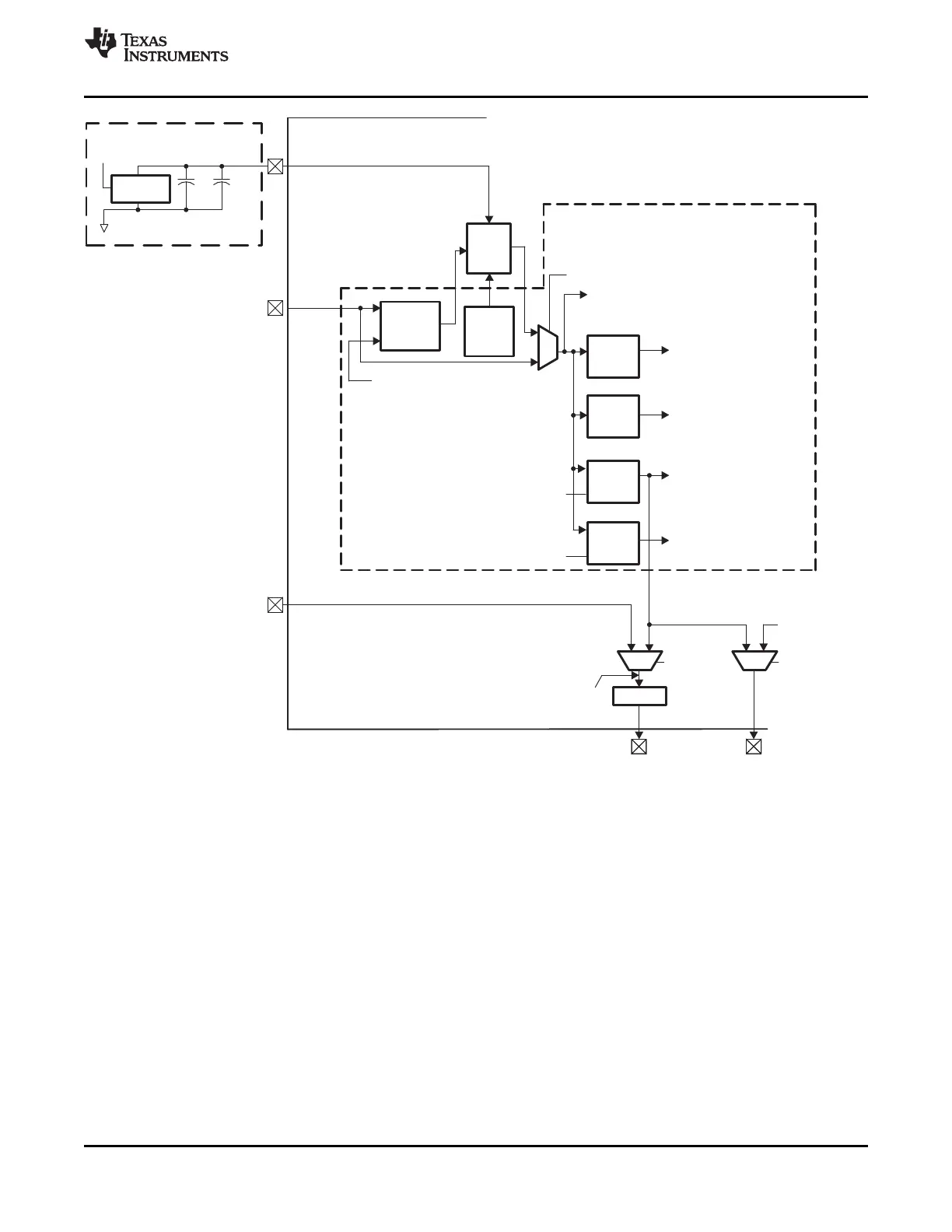
Figure 7-10. PLL1 and PLL1 Controller
7.7.1 PLL1 Controller Device-Specific Information
7.7.1.1 Internal Clocks and Maximum Operating Frequencies
As shown in Figure 7-10, the PLL1 controller generates several internal clocks including the system
reference clock (SYSREFCLK), and the system clocks (SYSCLK2/3/4/5). The high-frequency clock signal
SYSREFCLK is directly used to clock the C64x+ megamodule (including the CPU) and also serves as a
reference clock for the rest of the DSP system.
Dividers D2, D3, D4, and D5 divide the high-frequency clock SYSREFCLK to generate SYSCLK2,
SYSCLK3, SYSCLK4, and SYSCLK5, respectively. The system clocks are used to clock different portions
of the DSP:
• SYSCLK2 is used to clock the switched central resources (SCRs), EDMA3, VCP2, TCP2, and
RapidIO, as well as the data bus interfaces of the EMIFA and DDR2 Memory Controller.
• SYSCLK3 clocks the PCI, HPI, UTOPIA, McBSP, GPIO, TIMER, and I2C peripherals, as well as the
configuration bus of the PLL2 Controller.
Copyright © 2005–2012, Texas Instruments Incorporated C64x+ Peripheral Information and Electrical Specifications 133
Submit Documentation Feedback
Product Folder Link(s): TMS320C6455