TMS320C6455
SPRS276M –MAY 2005–REVISED MARCH 2012
www.ti.com
• SYSCLK4 is used as the internal clock for the EMIFA. It is also used to clock other logic within the
DSP.
• SYSCLK5 clocks the emulation and trace logic of the DSP.
The divider ratio bits of dividers D2 and D3 are fixed at ÷3 and ÷6, respectively. The divider ratio bits of
dividers D4 and D5 are programmable through the PLL controller divider registers PLLDIV4 and PLLDIV5,
respectively.
The PLL multiplier controller (PLLM) and the dividers (D4 and D5) must be programmed after reset. There
is no hardware CLKMODE selection on the C6455 device.
Since the divider ratio bits for dividers D2 and D3 are fixed, the frequency of SYSCLK2 and SYSCLK3 is
tied to the frequency of SYSREFCLK. However, the frequency of SYSCLK4 and SYSCLK5 depends on
the configuration of dividers D4 and D5. For example, with PLLM in the PLL1 multiply control register set
to 10011b (x20 mode) and a 50-MHz CLKIN1 input, the PLL output PLLOUT is set to 1000 MHz and
SYSCLK2 and SYSCLK3 run at 333 MHz and 166 MHz, respectively. Divider D4 can be programmed
through the PLLDIV4 register to divide SYSREFCLK by 10 such that SYSCLK4 and, hence, the EMIF
internal clock, runs at 120 MHz.
All hosts (HPI, PCI, etc.) must hold off accesses to the DSP while the frequency of its internal clocks is
changing. A mechanism must be in place such that the DSP notifies the host when the PLL configuration
has completed.
Note that there is a minimum and maximum operating frequency for PLLREF, PLLOUT, SYSCLK4, and
SYSCLK5. The PLL1 Controller must not be configured to exceed any of these constraints (certain
combinations of external clock input, internal dividers, and PLL multiply ratios might not be supported). For
the PLL clocks input and output frequency ranges, see Table 7-16.
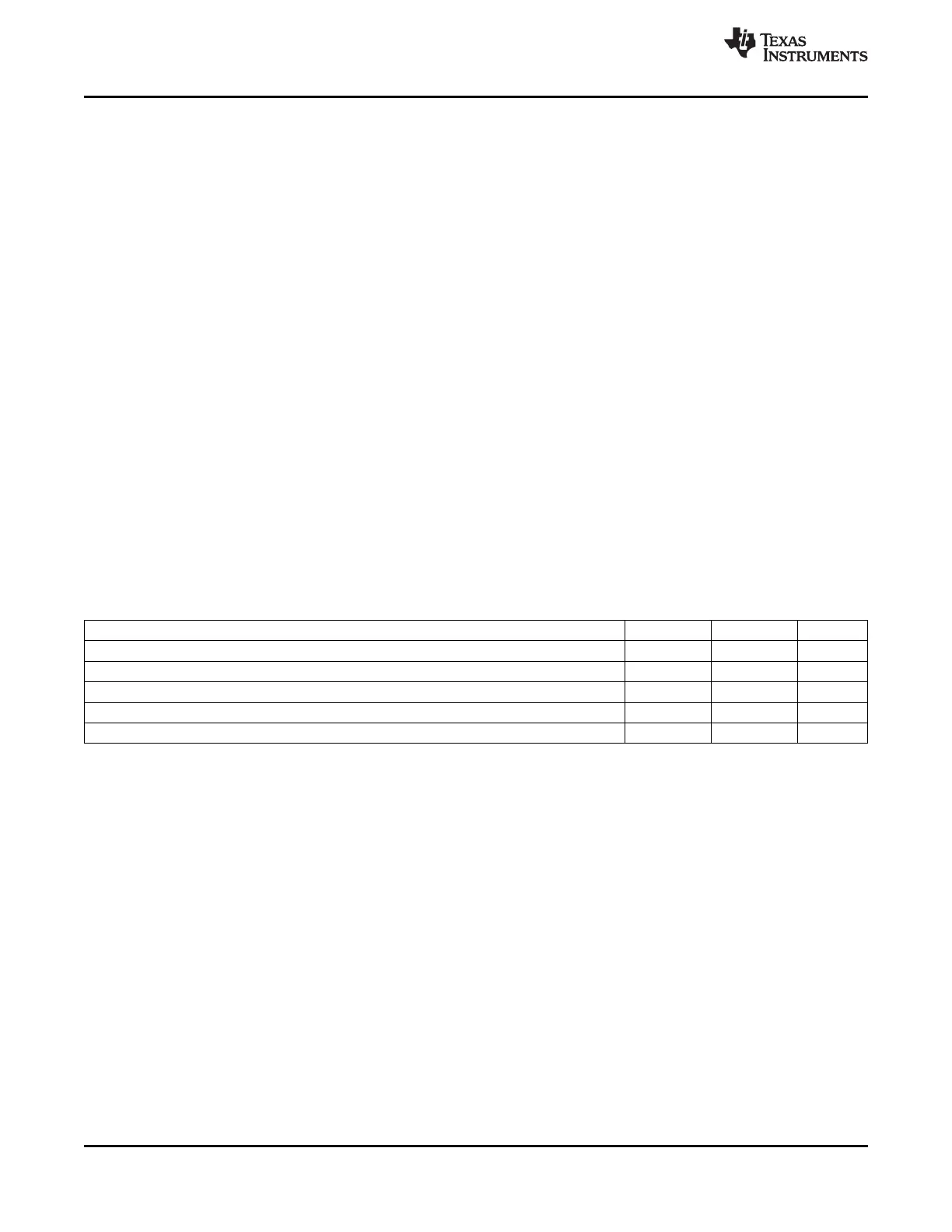
Table 7-16. PLL1 Clock Frequency Ranges
CLOCK SIGNAL MIN MAX UNIT
CLKIN1 66.6 MHz
PLLREF (PLLEN = 1)
(1)
33.3 66.6 MHz
PLLOUT
(1)
400 1200 MHz
SYSCLK4 25 166 MHz
SYSCLK5 333 MHz
(1) Only applies when the PLL1 Controller is set to PLL mode (PLLEN = 1 in the PLLCTL register).
7.7.1.2 PLL1 Controller Operating Modes
The PLL1 controller has two modes of operation: bypass mode and PLL mode. The mode of operation is
determined by the PLLEN bit of the PLL control register (PLLCTL). In PLL mode, SYSREFCLK is
generated from the device input clock CLKIN1 using the divider PREDIV and the PLL multiplier PLLM. In
bypass mode, CLKIN1 is fed directly to SYSREFCLK.
All hosts (HPI, PCI, etc.) must hold off accesses to the DSP while the frequency of its internal clocks is
changing. A mechanism must be in place such that the DSP notifies the host when the PLL configuration
has completed.
7.7.1.3 PLL1 Stabilization, Lock, and Reset Times
The PLL stabilization time is the amount of time that must be allotted for the internal PLL regulators to
become stable after device powerup. The PLL should not be operated until this stabilization time has
expired.
The PLL reset time is the amount of wait time needed when resetting the PLL (writing PLLRST = 1), in
order for the PLL to properly reset, before bringing the PLL out of reset (writing PLLRST = 0). For the
PLL1 reset time value, see Table 7-17.
134 C64x+ Peripheral Information and Electrical Specifications Copyright © 2005–2012, Texas Instruments Incorporated
Submit Documentation Feedback
Product Folder Link(s): TMS320C6455