TMS320C6455
www.ti.com
SPRS276M –MAY 2005–REVISED MARCH 2012
7.21 General-Purpose Input/Output (GPIO)
7.21.1 GPIO Device-Specific Information
On the C6455 device, the GPIO peripheral pins GP[15:8] and GP[3:0] are muxed with the UTOPIA, PCI,
and McBSP1 peripheral pins and the SYSCLK4 signal. For more detailed information on device/peripheral
configuration and the C6455 device pin muxing, see Section 3, Device Configuration.
7.21.2 GPIO Peripheral Register Descriptions
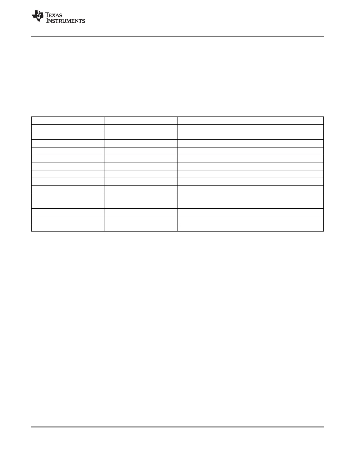
Table 7-113. GPIO Registers
HEX ADDRESS RANGE ACRONYM REGISTER NAME
02B0 0008 BINTEN GPIO interrupt per bank enable register
02B0 000C - Reserved
02B0 0010 DIR GPIO Direction Register
02B0 0014 OUT_DATA GPIO Output Data register
02B0 0018 SET_DATA GPIO Set Data register
02B0 001C CLR_DATA GPIO Clear Data Register
02B0 0020 IN_DATA GPIO Input Data Register
02B0 0024 SET_RIS_TRIG GPIO Set Rising Edge Interrupt Register
02B0 0028 CLR_RIS_TRIG GPIO Clear Rising Edge Interrupt Register
02B0 002C SET_FAL_TRIG GPIO Set Falling Edge Interrupt Register
02B0 0030 CLR_FAL_TRIG GPIO Clear Falling Edge Interrupt Register
02B0 008C - Reserved
02B0 0090 - 02B0 00FF - Reserved
02B0 0100 - 02B0 3FFF - Reserved
Copyright © 2005–2012, Texas Instruments Incorporated C64x+ Peripheral Information and Electrical Specifications 245
Submit Documentation Feedback
Product Folder Link(s): TMS320C6455