TMS320C6455
www.ti.com
SPRS276M –MAY 2005–REVISED MARCH 2012
2 Device Overview
2.1 Device Characteristics
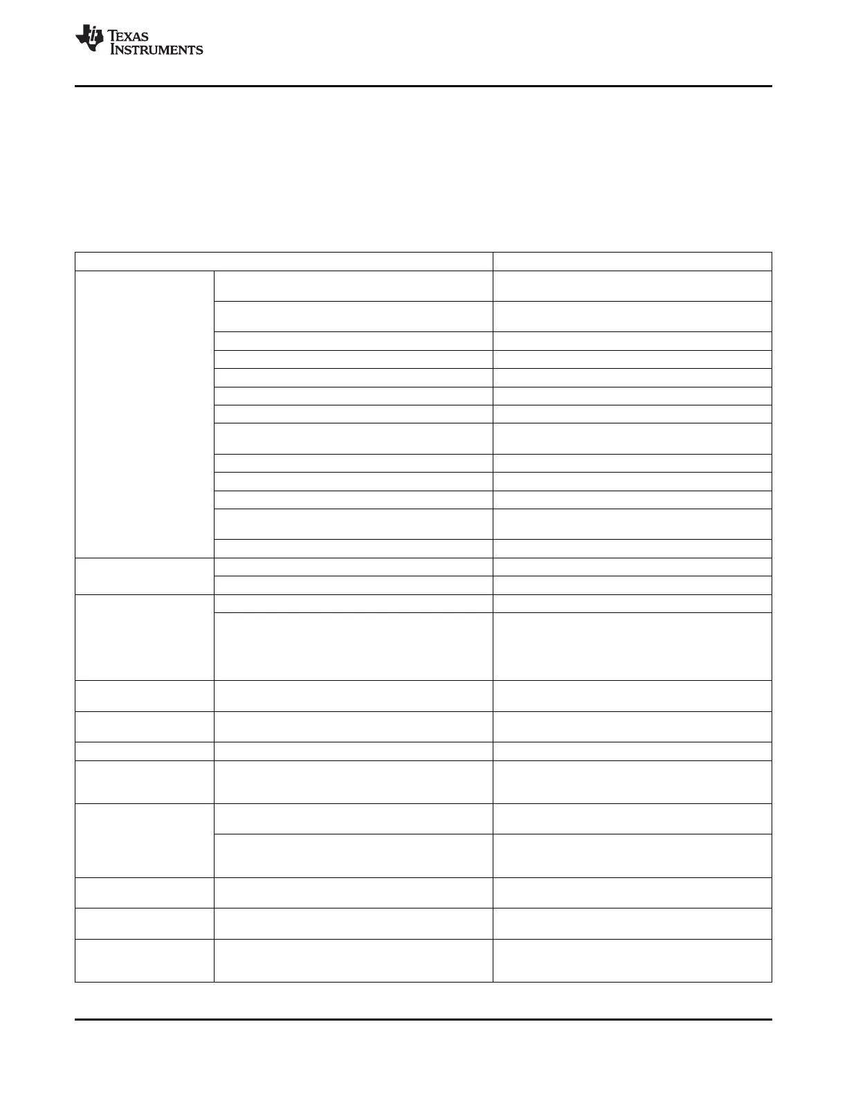
Table 2-1, provides an overview of the C6455 DSP. The tables show significant features of the C6455
device, including the capacity of on-chip RAM, the peripherals, the CPU frequency, and the package type
with pin count.
Table 2-1. Characteristics of the C6455 Processor
HARDWARE FEATURES C6455
EMIFA (64-bit bus width)
1
(clock source = AECLKIN or SYSCLK4)
DDR2 Memory Controller (32-bit bus width) [1.8 V I/O]
1
(clock source = CLKIN2)
EDMA3 (64 independent channels) [CPU/3 clock rate] 1
High-speed 1x/4x Serial Rapid IO Port 1
I2C 1
Peripherals
HPI (32- or 16-bit user selectable) 1 (HPI16 or HPI32)
Not all peripherals pins
are available at the same
PCI (32-bit), [66-MHz or 33-MHz] 1 (PCI66 or PCI33)
time (For more detail, see
McBSPs (internal CPU/6 or external clock source up
Section 3, Device
2
to 100 Mbps)
Configuration).
UTOPIA (8-bit mode, 50-MHz, Slave-only) 1
10/100/1000 Ethernet MAC (EMAC) 1
Management Data Input/Output (MDIO) 1
64-Bit Timers (Configurable)
2 64-bit or 4 32-bit
(internal clock source = CPU/6 clock frequency)
General-Purpose Input/Output Port (GPIO) 16
VCP2 (clock source = CPU/3 clock frequency) 1
Decoder Coprocessors
TCP2 (clock source = CPU/3 clock frequency) 1
Size (Bytes) 2192K
32K-Byte (32KB) L1 Program Memory Controller
[SRAM/Cache]
On-Chip Memory
Organization 32KB Data Memory Controller [SRAM/Cache]
2048KB L2 Unified Memory/Cache
32KB L2 ROM
C64x+ Megamodule Megamodule Revision ID Register (address location:
See Section 5.6, Megamodule Revision
Revision ID 0181 2000h)
See Section 3.6, JTAG ID (JTAGID) Register
JTAG BSDL_ID JTAGID register (address location: 0x02A80008)
Description
Frequency MHz 720, 850, 1000 (1 GHz), and 1200 (1.2 GHz)
1.39 ns (C6455-720), 1.17 ns (C6455-850),
Cycle Time ns 1 ns (C6455 A-1000, -1000) [1-GHz CPU]
(1)
0.83 ns (C6455-1200) [1.2-GHz CPU]
1.25 V (A-1000/-1000/-1200)
Core (V)
1.2 V (-850/-720)
Voltage
1.25/1.2 [RapidIO],
I/O (V) 1.5/1.8 [EMAC RGMII], and
1.8 and 3.3 V [I/O Supply Voltage]
PLL1 and PLL1
CLKIN1 frequency multiplier Bypass (x1), x15, x20, x25, x30, x32
Controller Options
CLKIN2 frequency multiplier
PLL2 x20
[DDR2 Memory Controller and EMAC support only]
697-Pin Flip-Chip Plastic BGA (CTZ)
BGA Package 24 x 24 mm 697-Pin Plastic BGA (GTZ)
697-Pin Flip-Chip Plastic BGA (ZTZ)
(1) The extended temperature device's (A-1000) electrical characteristics and ac timings are the same as those for the corresponding
commercial temperature devices (-1000).
Copyright © 2005–2012, Texas Instruments Incorporated Device Overview 7
Submit Documentation Feedback
Product Folder Link(s): TMS320C6455