Port Integration Module (PIM)
MFR4310 Reference Manual, Rev. 2
208 Freescale Semiconductor
4.2.1 Functional Mode
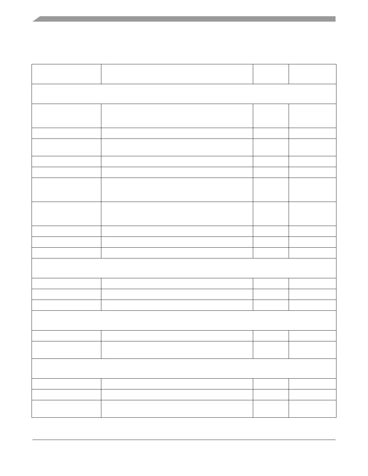
Table 4-1. Pin Functions (Functional Mode)
Name Function Direction
Special
Configuration
1
Host Interface
A[6:1]/XADDR[14:19] AMI/MPC address bus; HCS12 expanded address lines.
A1 is the LSB of the AMI/MPC address bus; XADDR14 is the
LSB of the HCS12 expanded address lines
Input PU/PD
A[7:9] AMI/MPC address bus Input PU/PD
OE#/ACS0 AMI/MPC read output enable signal; HCS12 address select
input
Input PU/PD
A[12:11]/ACS[2:1] AMI/MPC address bus; HCS12 address select inputs Input PU/PD
BSEL[1:0]#/DBG[0:1] AMI/MPC byte select; Debug strobe point Input/Output DC/PU/PD
D[15:8]/PB[0:7] AMI/MPC data bus; HCS12 multiplexed address/data bus.
D15 is the MSB of the AMI/MPC data bus; PB0 is the LSB of
the HCS12 address/data bus
Input/Output DC/PU/PD
D[7:0]/PA[0:7] AMI/MPC data bus; HCS12 multiplexed address/data bus.
D0 is the LSB of the AMI/MPC data bus; PA7 is the MSB of the
HCS12 address/data bus
Input/Output DC/PU/PD
CE#/LSTRB AMI/MPC chip select signal; HCS12 low-byte strobe signal Input PU/PD
WE#/RW_CC# AMI write enable signal; HCS12 read/write select signal Input PU/PD
A10/ECLK_CC AMI/MPC address bus/; HCS12 clock input Input PU/PD
Physical Layer Interface
RXD_BG[2:1] PHY Data receiver input Input PU/PD
TXEN[2:1]# Transmit enable for PHY Output DC
TXD_BG[1:2]/IF_SEL[1:0] PHY Data transmitter output / Host interface select Input/Output DC
Clock Interface
CHICLK_CC External CHI clock input selectable Input -
CLKOUT Controller clock output selectable between disabled,
4/10/40 MHz
Output DC
Other
RESET# Hardware reset input Input PD
INT_CC# Controller interrupt output Output DC/OD
TEST Factory Test mode select — must be tied to logic low in
application
Input PD