Device Overview
MFR4310 Reference Manual, Rev. 2
Freescale Semiconductor 35
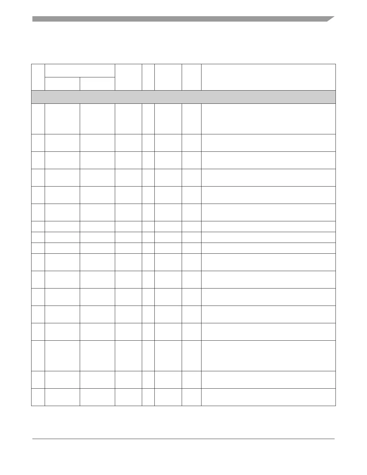
2.4.2 Pin Functions and Signal Properties
Table 2-3. Pin Functions and Signal Properties
Pin
#
Pin Name
1
Powered
by
I/O
Pin
Type
2, 3
Reset Functional Description
Function 1 Function 2
Host Interface Pins
11 A1 XADDR19 VDDX I PC - AMI/MPC address bus;
HCS12 expanded address lines.
A1 is the LSB of the AMI/MPC address bus; XADDR14
is the LSB of the HCS12 expanded address lines
12 A2 XADDR18 VDDX I PC - AMI/MPC address bus;
HCS12 expanded address lines.
13 A3 XADDR17 VDDX I PC - AMI/MPC address bus;
HCS12 expanded address lines.
14 A4 XADDR16 VDDX I PC - AMI/MPC address bus;
HCS12 expanded address lines.
15 A5 XADDR15 VDDX I PC - AMI/MPC address bus;
HCS12 expanded address lines.
17 A6 XADDR14 VDDX I PC - AMI/MPC address bus;
HCS12 expanded address lines.
18 A7 - VDDX I PC - AMI/MPC address bus
21 A8 - VDDX I PC - AMI/MPC address bus
22 A9 - VDDX I PC - AMI/MPC address bus
27 OE# ACS0 VDDX I PC - AMI/MPC read output enable signal;
HCS12 address select input
28 A11 ACS1 VDDX I PC - AMI/MPC address bus;
HCS12 address select inputs
34 A12 ACS2 VDDX I PC - AMI/MPC address bus;
HCS12 address select inputs
48 BSEL1# DBG0 VDDX I/O PC - AMI/MPC byte select;
Debug strobe point
47 BSEL0# DBG1 VDDX I/O PC - AMI/MPC byte select;
Debug strobe point
10 D15 PB0 VDDX I/O Z/DC/PC Z AMI/MPC data bus;
HCS12 multiplexed address/data bus.
D15 is the MSB of the AMI/MPC data bus; PB0 is the
LSB of the HCS12 address/data bus
7 D14 PB1 VDDX I/O Z/DC/PC Z AMI/MPC data bus;
HCS12 multiplexed address/data bus
6 D13 PB2 VDDX I/O Z/DC/PC Z AMI/MPC data bus;
HCS12 multiplexed address/data bus