Printed Circuit Board Layout Recommendations
MFR4310 Reference Manual, Rev. 2
Freescale Semiconductor 261
Appendix C
Printed Circuit Board Layout Recommendations
The PCB must be laid out carefully to ensure proper operation of the voltage regulator and the CC. The
following rules must be observed:
• Every supply pair must be decoupled by a ceramic capacitor connected as near as possible to the
corresponding pins (Cd).
• The central point of the ground star should be the VSSR pin.
• Low-ohmic low-inductance connections should be used between VSSX and VSSR.
• VSSOSC must be directly connected to VSSR.
• Traces of VSSOSC, EXTAL and XTAL must be kept as short as possible. Occupied board area for
C1, C2, C3 and Q should be as small as possible.
• Other signals or supply lines should not be routed under the area occupied by C1, C2, C3, and Q
and the connection area of the CC.
• The central power input should be fed in at the VDDA/VSSA pins.
Figure C-1 shows a recommended PCB layout (64-pin LQFP) for standard Pierce oscillator mode, while
Table C-1 provides suggested values for the external components.
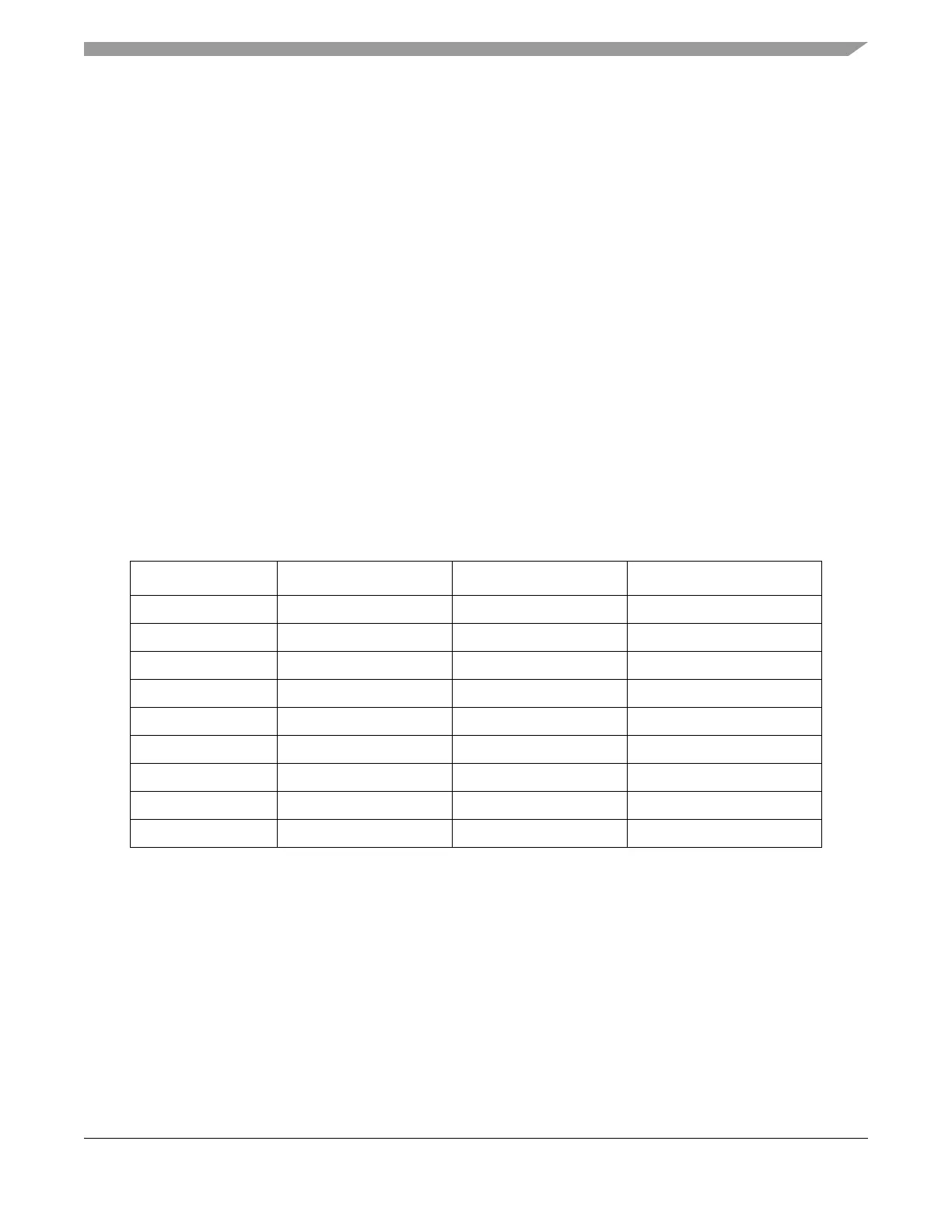
Table C-1. Suggested External Component Values
Component Purpose Type Value
C1 OSC load cap ceramic X7R 2pF
C2 OSC load cap ceramic X7R 2pF
C3 VDDOSC filter cap ceramic X7R 100– 220nF
C4 VDDA filter cap ceramic X7R 100– 220nF
Cd VDDR, VDDX filter cap ceramic X7R/tantalum 100– 220nF
Cload VDD2_5 filter cap ceramic X7R 100– 220nF
R
B
OSC resistance 1 MΩ
R
S
OSC resistance 0 Ω (i.e. short-circuit)
Q Quartz NDK NX8045GA 40 MHz