Dual Output Voltage Regulator (VREG3V3V2)
MFR4310 Reference Manual, Rev. 2
Freescale Semiconductor 219
5.2 External Signal Description
Due to the nature of VREG3V3V2 being a voltage regulator providing the chip internal power supply
voltages most signals are power supply signals connected to pads.
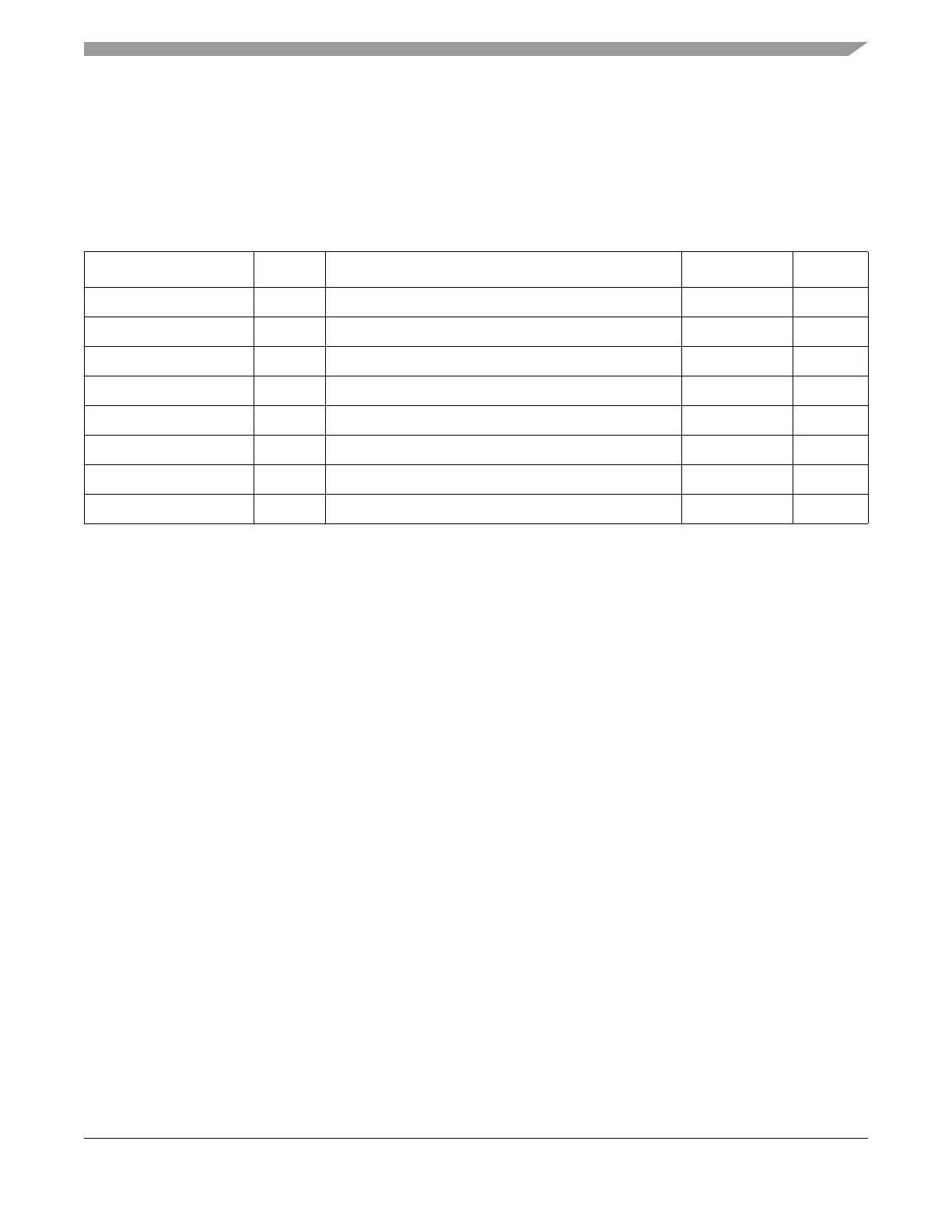
Table 5-1 shows all signals of VREG3V3V2 associated with pins.
NOTE
Check device overview chapter for connectivity of the signals.
5.2.1 V
DDR
, V
SSR
— Regulator Power Input
Signal V
DDR
is the power input of VREG3V3V2. All currents sourced into the regulator loads flow
through this pin. A chip external decoupling capacitor (100 nF…220 nF, X7R ceramic) between V
DDR
and
V
SSR
can smoothen ripple on V
DDR
.
For entering shutdown mode, pin V
DDR
must be tied to ground. In that case, V
DD2_5
/V
SS2_5
and
V
DDOSC
/V
SSOSC
must be provided externally.
5.2.2 V
DDA
, V
SSA
— Regulator Reference Supply
Signals V
DDA
/V
SSA
which are supposed to be relatively quiet are used to supply the analog parts of the
regulator. Internal precision reference circuits are supplied from these signals. A chip external decoupling
capacitor (100 nF…220 nF, X7R ceramic) between V
DDA
and V
SSA
can further improve the quality of this
supply.
Table 5-1. VREG3V3V2 — Signal Properties
Name Port Function Reset State Pullup
V
DDR
— VREG3V3V2 power input (positive supply) — —
V
SSR
— VREG3V3V2 power input (ground) — —
V
DDA
— VREG3V3V2 quiet input (positive supply) — —
V
SSA
— VREG3V3V2 quiet input (ground) — —
V
DD2_5
— VREG3V3V2 primary output (positive supply) — —
V
SS2_5
— VREG3V3V2 primary output (ground) — —
V
DDOSC
— VREG3V3V2 secondary output (positive supply) — —
V
SSOSC
— VREG3V3V2 secondary output (ground) — —