Device Overview
MFR4310 Reference Manual, Rev. 2
Freescale Semiconductor 51
— The chip enable CE#, the output enable OE#, and the write enables BSEL[1:0]# are used to
determine the type of access as shown in Table 2-8.
• BSEL[1:0]# inputs indicate the direction of the data transfer for a transaction.
• OE# input enables the MPC data output during read transactions.
NOTE
D0 is the LSB of the 16-bit data bus.
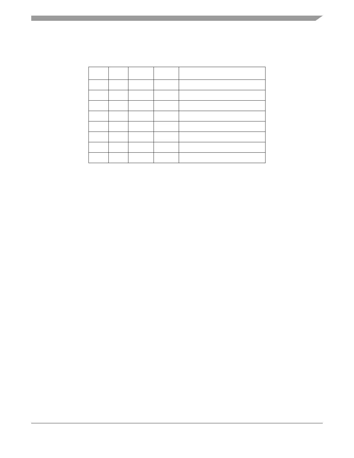
Table 2-9. MPC Interface Access Types
CE# OE# BSEL1# BSEL0# Type of Access
0 0 X 0 illegal
0 0 0 X illegal
0 0 1 1 16-bit read from word address
1
1
Read data from even byte address at D[15:8] and from odd byte address at
D[7:0].
0 1 0 0 16-bit write to word address
2
2
Write data from D[15:8] to even byte address and from D[7:0] to odd byte
address.
0 1 0 1 8-bit write to even byte address
3
3
Write data from D[15:8].
0 1 1 0 8-bit write to odd byte address
4
4
Write data from D[7:0].
0 1 1 1 no access
1 X X X no access