PIM Memory Map and Registers
MFR4310 Reference Manual, Rev. 2
Freescale Semiconductor 209
The TEST and RESET pads have internal pulldown resistors, where the pulldown resistor on RESET is
disabled when TEST is asserted. If the RESET pad gets disconnected, the device goes into a safe state
(reset mode).
4.2.2 Reset Mode
This pin configuration is enabled in reset mode only. Refer to Chapter 6, “Clocks and Reset Generator
(CRG)” for reset mode details. When the device is in reset mode, the corresponding pads go into input
mode with pull enabled.
4.3 PIM Memory Map and Registers
This section provides a detailed description of all registers in the Port Integration Module.
Only 16-bit reads and 8-bit and 16-bit writes are allowed to all registers.
DBG[3:2]/CLK_S[1:0] Debug strobe point / External CHI clock input select Output DC
Oscillator
EXTAL/CC_CLK Crystal driver / External clock Input -
XTAL Crystal driver Input -
1
Acronyms:
PC – (Pullup/pulldown Controlled) Register controlled internal weak pullup/pulldown for a pin in the input mode
PU/PD – (Pullup/pulldown) Internal weak pullup/pulldown for a pin in the input mode
DC – (Drive strength Controlled) Register controlled drive strength for a pin in the output mode
Table 4-2. Pin Functions (Reset Mode)
Name Direction Special Configuration
1
1
Acronyms:
PU/PD – (Pullup/pulldown) Internal weak pullup/pulldown for a pin in the input mode
TXD_BG2/IF_SEL0 Input PU
TXD_BG1/IF_SEL1 Input PD
DBG[3:2]/CLK_S[1:0] Input PD
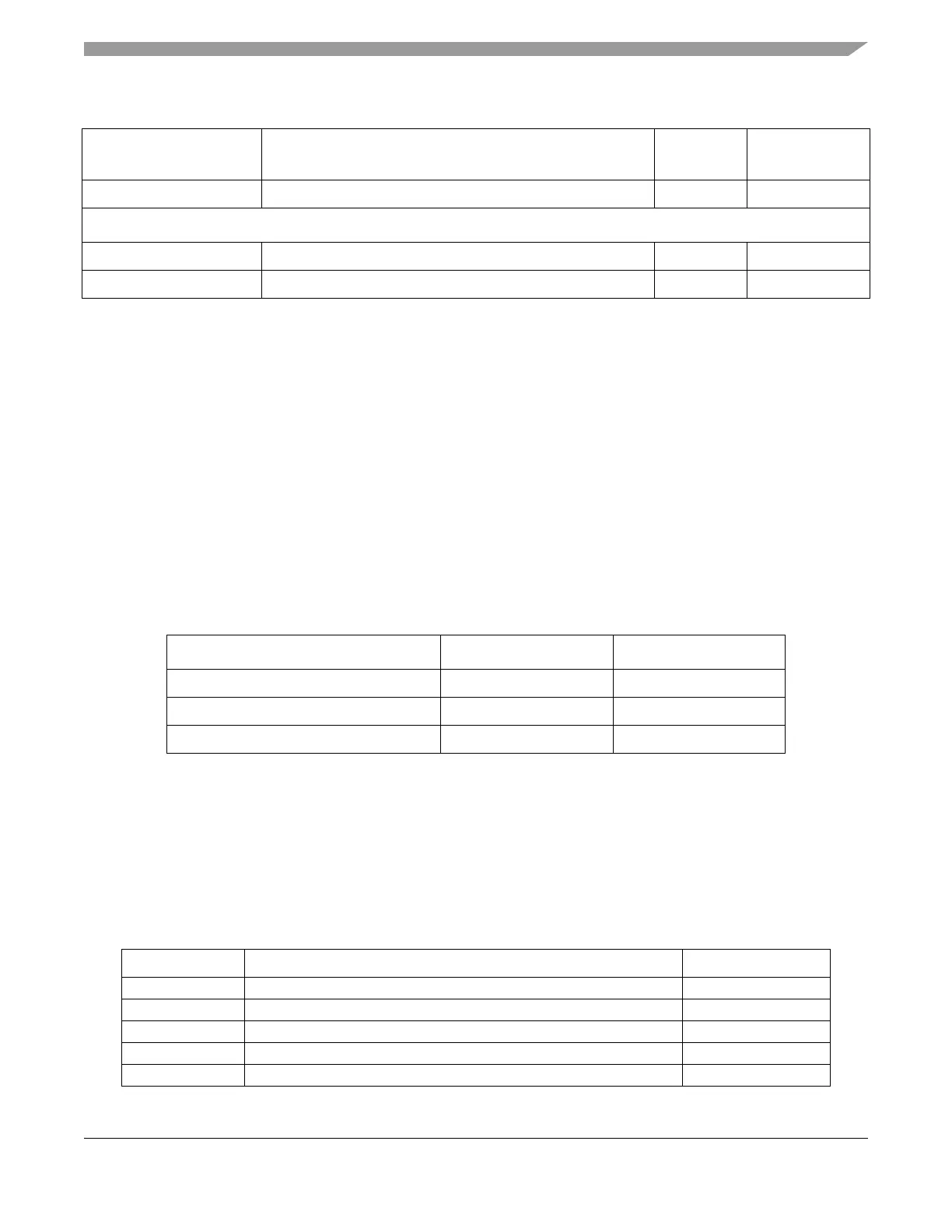
Table 4-3. Port Integration Module Memory Map
Address Use Access
0x00F0 Part ID Register (PIDR) R
0x00F2 ASIC Version Number Register (AVNR) R
0x00F4 Host Interface Pins Drive Strength Register (HIPDSR) R/W
0x00F6 Physical Layer Pins Drive Strength Register (PLPDSR) R/W
0x00F8 Host Interface Pins Pullup/pulldown Enable Register (HIPPER) R/W
Table 4-1. Pin Functions (Functional Mode) (continued)
Name Function Direction
Special
Configuration
1