Clocks and Reset Generator (CRG)
MFR4310 Reference Manual, Rev. 2
Freescale Semiconductor 225
NOTE
After reset, the clock monitor mechanism is disabled.
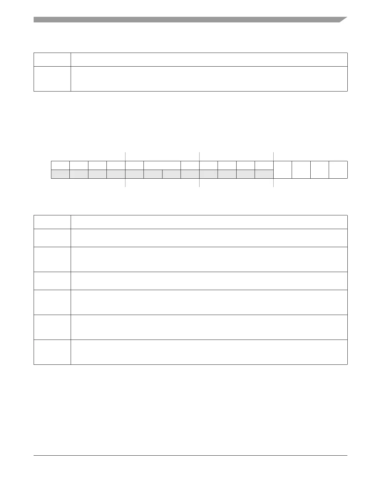
6.3.2 Clock and Reset Status Register (CRSR)
NOTE
On a power-on or low-voltage reset, CMIF and PRIF are both cleared to 0.
Table 6-2. DER Field Descriptions
Field Description
0
CMIE
Clock Monitor Mechanism Enable
0 Clock monitor mechanism disabled
1 Clock monitor mechanism enabled
Address in MFR4310 = 0x00E2 Write: Any Time
1514131211109876543210
R00000 CDCV ECS 0 0 0 0
ERIF PRIF CMIF LVIF
W
Reset000000000000––––
Figure 6-2. Clock and Reset Status Register (CRSR)
Table 6-3. CRSR Field Descriptions
Field Description
0
LVIF
Low Voltage Reset Interrupt Flag — set when a low-voltage reset has occurred.
Cleared by writing a 1. Writing 0 has no effect.
1
CMIF
Clock Monitor Reset Interrupt Flag — set when a clock monitor reset has occurred.
Cleared by writing a 1. Writing 0 has no effect.
Note: If LVIF bit or PRIF bit is set to 1 then the CMIF bit value is 0.
2
PRIF
Power-on Reset Interrupt Flag — set when a power-on reset has occurred.
Cleared by writing a 1. Writing 0 has no effect.
3
ERIF
External Reset Interrupt Flag — set when a external reset has occurred.
Cleared by writing a 1. Writing 0 has no effect.
Note: If LVIF bit or PRIF bit is set to 1 then the ERIF bit value is 0.
8
ECS
CHI Clock Source
0 CHI blocks are clocked by EXTAL
1 CHI blocks are clocked by CHICLK_CC
10-9
CDCV
CLKOUT Division Control Value — contains sampled value of CLK_S[1:0]. The CRG writes this value after a
power-on, low-voltage or clock monitor reset, according to the values sampled on the CLK_S[1:0] pins.
See Ta bl e 2 -5 for coding.