Device Overview
MFR4310 Reference Manual, Rev. 2
Freescale Semiconductor 45
2.4.4.3 VDD2_5, VSS2_5 — Core Power Pins
Power is supplied to the MFR4310 core through VDD2_5 and VSS2_5. This 2.5 V supply is derived from
the internal voltage regulator. No static load is allowed on these pins. If VDDR is tied to ground, the
internal voltage regulator is turned off.
NOTE
No load is allowed except for bypass capacitors.
2.4.4.4 VDDA, VSSA — Power Supply Pins for VREG
VDDA, VSSA are the power supply and ground input pins for the voltage regulator. They also provide the
reference voltages for the internal voltage regulator.
2.4.4.5 VDDOSC, VSSOSC — Power Supply Pins for OSC
VDDOSC, VSSOSC provide operating voltage and ground for the oscillator. This allows the supply
voltage to the oscillator to be bypassed independently. This 2.5 V voltage is generated by the internal
voltage regulator.
NOTE
No load is allowed except for bypass capacitors.
2.5 Modes of Operation
Refer to Section 3.1.6, “Modes of Operation” for full descriptions of the MFR4310 Disabled and Normal
modes of operation.
2.6 External Clock and Host Interface Selection
2.6.1 External 4/10/40 MHz Output Clock
A continuous external 4/10/40 MHz output clock signal is provided by the CC on the CLKOUT pin. See
Section 2.4.3.15, “CLKOUT — Clock Output” for details of when this signal is active.
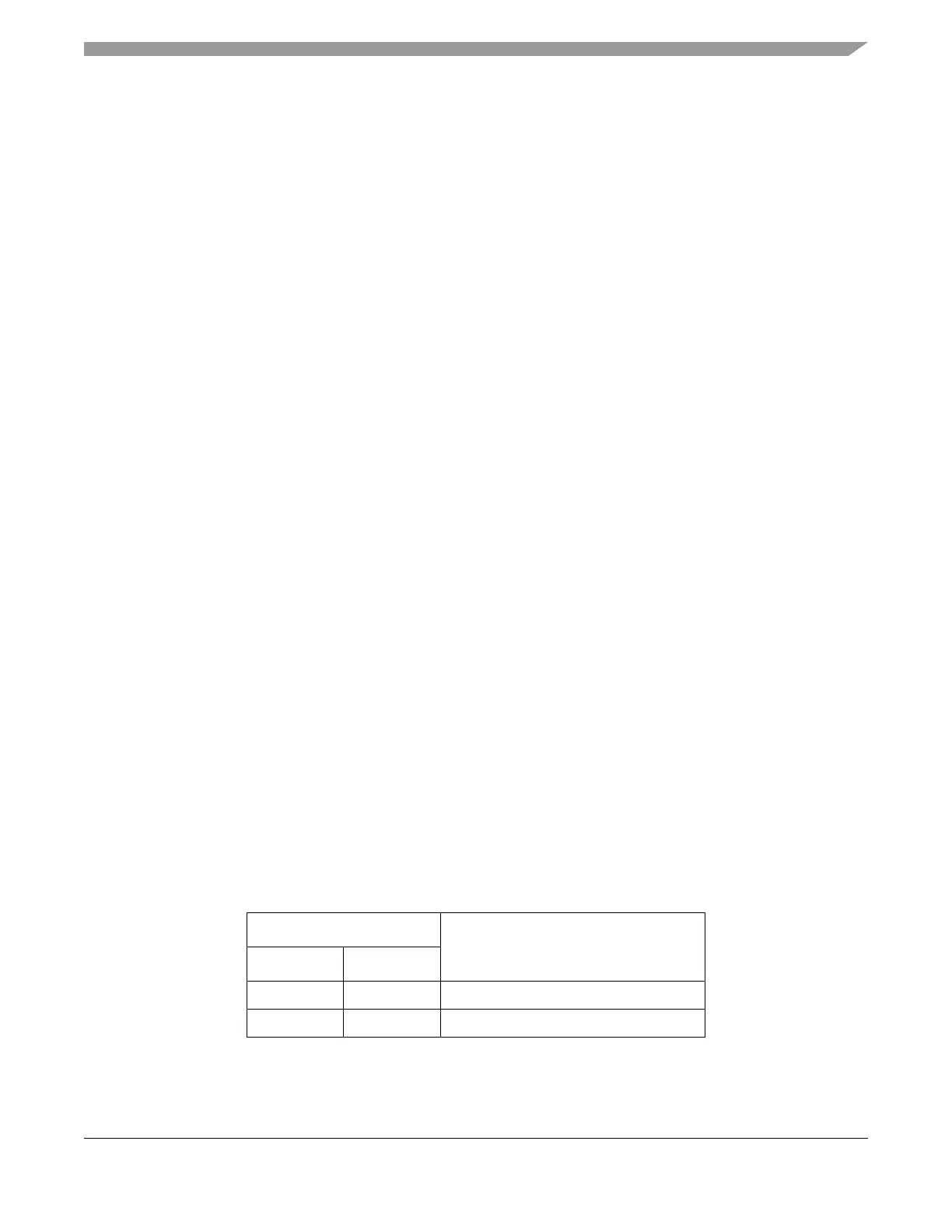
The output frequency of the CLKOUT signal is selected by the CLK_S[1:0] input pins, in accordance with
Table 2-5:
Table 2-5. CLKOUT Frequency Selection
Pin
CLKOUT Function
CLK_S0 CLK_S1
0 0 4 MHz output
1
1 0 10 MHz output