Electrical Characteristics
MFR4310 Reference Manual, Rev. 2
Freescale Semiconductor 251
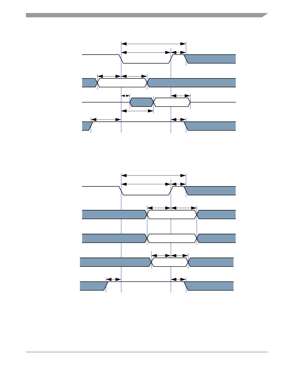
Figure A-2. AMI Interface Read Timing Diagram
Figure A-3. AMI Interface Write Timing Diagram
FUNC1
A[12:1] ADDRESS
t
SAR
D[15:0] DATA
t
HAR
t
LZOE
t
HZOE
t
HOE
t
RC
t
DOE
t
LOE
WE#
t
WEOE
t
OEWE
Note: The signal FUNC1 is a logical OR of the chip enable (CE#) and output enable (OE#) inputs.
FUNC2
A[12:1] ADDRESS
t
SAW
D[15:0] DATA
t
HAW
t
SD
t
HD
t
WC
OE#
t
HWE
t
LWE
t
WEOE
t
OEWE
BSEL[1:0]# BYTE SELECT
Note: The signal FUNC2 is a logical OR of the chip enable (CE#) and write enable (WE#) inputs.