Electrical Characteristics
MFR4310 Reference Manual, Rev. 2
Freescale Semiconductor 253
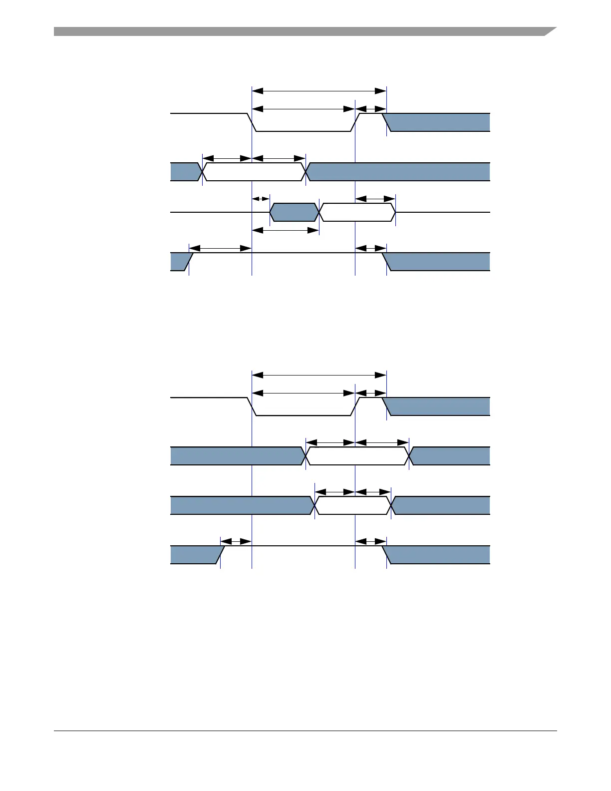
Figure A-4. MPC Interface Read Timing Diagram
Figure A-5. MPC Interface Write Timing Diagram
FUNC3
A[12:1] ADDRESS
t
SAR
D[15:0] DATA
t
HAR
t
LZOE
t
HZOE
t
HOE
t
RC
t
DOE
t
LOE
BSEL[1:0]#
t
BSELOE
t
OEBSEL
Note: The signal FUNC3 is a logical OR of the chip enable (CE#) and output enable (OE#) inputs.
FUNC4
A[12:1] ADDRESS
t
SAW
D[15:0] DATA
t
HAW
t
SD
t
HD
t
WC
OE#
t
HBSEL
t
LBSEL
t
BSELOE
t
OEBSEL
Note: The signal FUNC4
is a logical OR of the chip enable (CE#) and the logically ANDed byte select (BSEL[1:0]#) inputs.