Electrical Characteristics
MFR4310 Reference Manual, Rev. 2
Freescale Semiconductor 239
injection current may flow out of VDD5 and could result in external power supply going out of regulation.
Ensure external V
DD5
load shunts current greater than maximum injection current. This is the greatest risk
when the CC is not consuming power; e.g. if no system clock is present, or if clock rate is very low which
would reduce overall power consumption.
A.1.5 Absolute Maximum Ratings
CAUTION
Long-term exposure to absolute maximum ratings may affect device
reliability, and permanent damage may occur if operate exceeding the
rating. The device should be operated under recommended operating
condition.
Absolute maximum ratings are stress ratings only. A functional operation under or outside those maxima
is not guaranteed. Stress beyond those limits may affect the reliability or cause permanent damage of the
device.
This device contains circuitry protecting against damage due to high static voltage or electrical fields;
however, it is advised that normal precautions be taken to avoid application of any voltages higher than
maximum-rated voltages to this high-impedance circuit. Reliability of operation is enhanced if unused
inputs are tied to an appropriate logic voltage level (V
SS5
or V
DD5
).
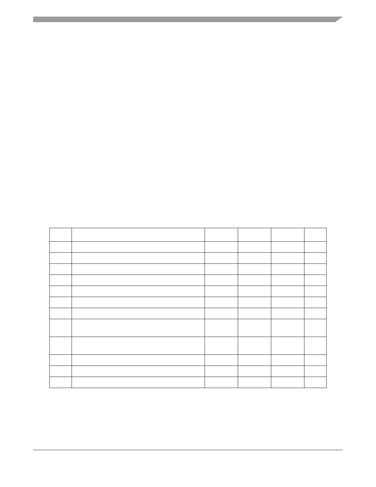
Table A-1. Absolute Maximum Ratings
Num Rating Symbol Min Max Unit
1 I/O, Regulator and Analog Supply Voltage V
DD5
-0.3 6.5 V
2 Digital Logic Supply Voltage
1
1
The device contains an internal voltage regulator to generate the logic and OSC supply out of the I/O supply. The
absolute maximum ratings apply when the device is powered from an external source.
V
DD
-0.3 3.0 V
3 Oscillator Supply Voltage
1
V
DDOSC
-0.3 3.0 V
4 Voltage difference VDDX to VDDR and VDDA Δ
VDDX
-0.3 0.3 V
5 Voltage difference VSSX to VSSR and VSSA Δ
VSSX
-0.3 0.3 V
6 Digital I/O Input Voltage
2
2
AC over or undershoots for ±2V beyond the supply if limited to 20ns length are allowed.
V
IN
-0.3 6.5 V
7 EXTAL, XTAL inputs V
ILV
-0.3 3.0 V
8 Instantaneous Maximum Current
Single pin limit for all digital I/O pins
3
3
All digital I/O pins are internally clamped to V
SSX
and V
DDX
, V
SSR
and V
DDR
or V
SSA
and V
DDA
.
I
D
-25 +25 mA
9 Instantaneous Maximum Current
Single pin limit for EXTAL, XTAL
4
4
Those pins are internally clamped to V
SSOSC
and V
DDOSC
.
I
DL
-25 +25 mA
10 Operating Temperature Range (packaged) T
A
-40 +125
o
C
11 Operating Temperature Range (junction) T
J
-40 +140
o
C
12 Storage Temperature Range T
stg
– 65 +155 °C