FlexRay Module (FLEXRAYV4)
MFR4310 Reference Manual, Rev. 2
Freescale Semiconductor 73
.;
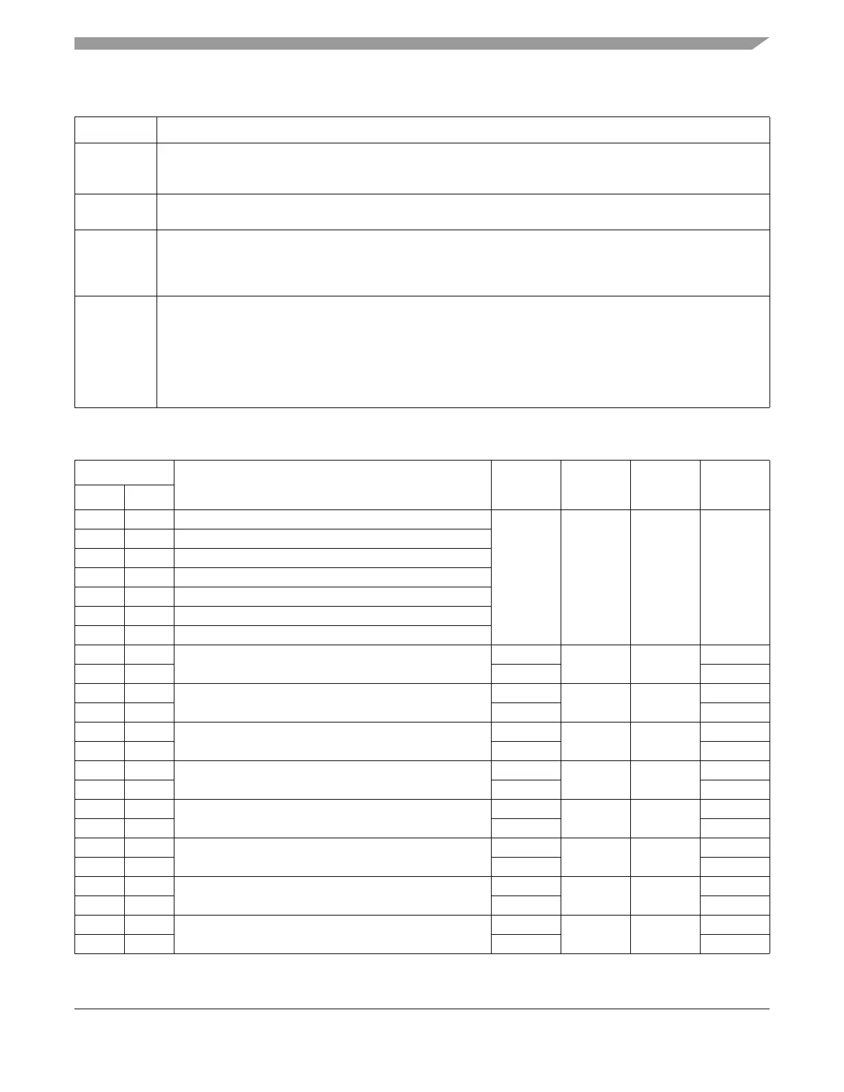
Table 3-11. STBSCR Field Descriptions
Field Description
15
WMD
Write Mode — This control bit defines the write mode of this register.
0 Write to all fields in this register on write access.
1 Write to SEL field only on write access.
14–8
SEL
Strobe Signal Select — This control field selects one of the strobe signals given in Tabl e 3 -1 2 to be enabled or
disabled and assigned to one of the four strobe ports given in Table 3- 12.
4
ENB
Strobe Signal Enable — The control bit is used to enable and to disable the strobe signal selected by
STBSSEL.
0 Strobe signal is disabled and not assigned to any strobe port.
1 Strobe signal is enabled and assigned to the strobe port selected by STBPSEL.
1–0
STBPSEL
Strobe Port Select — This field selects the strobe port that the strobe signal selected by the SEL is assigned
to. All strobe signals that are enabled and assigned to the same strobe port are combined with a binary OR
operation.
00 assign selected signal to DBG0
01 assign selected signal to DBG1
10 assign selected signal to DBG2
11 assign selected signal to DBG3
Table 3-12. Strobe Signal Mapping
SEL
Description Channel Type Offset
1
Reference
dec hex
0 0x00 poc_startup_state[0] (for coding see PSR0[4])
- value 0 MT start
1 0x01 poc_startup_state[1] (for coding see PSR0[5])
2 0x02 poc_startup_state[2] (for coding see PSR0[6])
3 0x03 poc_startup_state[3] (for coding see PSR0[7])
4 0x04 poc_state[0] (for coding see PSR0[8])
5 0x05 poc_state[1] (for coding see PSR0[9])
6 0x06 poc_state[2] (for coding see PSR0[10])
7 0x07
channel idle indicator
A
level +5
RXD_BG1
8 0x08 B RXD_BG2
9 0x09
receive data after glitch filtering
A
value +4
RXD_BG1
10 0x0A B RXD_BG2
11 0x0B
synchronization edge strobe
A
pulse +4
RXD_BG1
12 0x0C B RXD_BG2
13 0x0D
header received
A
pulse +4
RXD_BG1
14 0x0E B RXD_BG2
15 0x0F
wakeup symbol decoded
A
pulse +5
RXD_BG1
16 0x10 B RXD_BG2
17 0x11
MTS or CAS symbol decoded
A
pulse +4
RXD_BG1
18 0x12 B RXD_BG2
19 0x13
frame decoded
A
pulse +4
RXD_BG1
20 0x14 B RXD_BG2
21 0x15
channel idle detected
A
pulse +4
RXD_BG1
22 0x16 B RXD_BG2