Device Overview
MFR4310 Reference Manual, Rev. 2
38 Freescale Semiconductor
2.4.3 Detailed Signal Descriptions
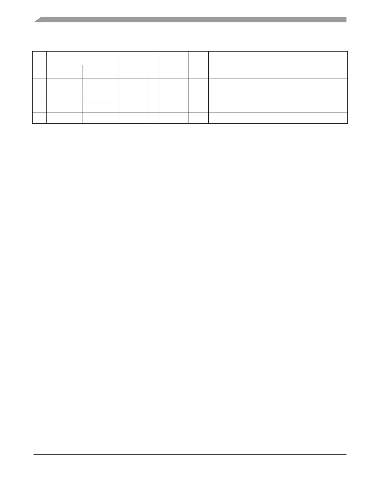
2.4.3.1 A[6:1]/XADDR[14:19] — AMI/MPC Address Bus; HCS12 Expanded
Address Inputs
A[6:1]/XADDR[14:19] are general purpose input pins. Their function is selected by the IF_SEL[1:0] pins.
Refer to Section 2.7, “External Host Interface” for more information. The pins can be configured to enable
or disable pullup or pulldown resistors on the pins. (See Section 4.3.1.5, “Host Interface Pins
Pullup/pulldown Enable Register (HIPPER)” and Section 4.3.1.6, “Host Interface Pins Pullup/pulldown
Control Register (HIPPCR)”.)
A[6:1] are AMI/MPC interface address signals. A1 is the LSB of the AMI/MPC address bus.
XADDR[14:19] are HCS12 interface expanded address lines. XADDR14 is the LSB of the HCS12
interface expanded address lines.
59 VDD2_5
4
- - - - - Core voltage power supply output (nominally 2.5V)
60 VSS2_5
4
- - - - - Core voltage ground output
26 VDDOSC
4
- - - - - Oscillator voltage power supply output (nominally 2.5V)
23 VSSOSC
4
- - - - - Oscillator voltage ground output
1
# – signal is active-low
2
Acronyms:
PC – (Pullup/pulldown Controlled) Register controlled internal weak pullup/pulldown for a pin in the input mode. Refer to the
following sections for more information:
– Section 4.3.1.5, “Host Interface Pins Pullup/pulldown Enable Register (HIPPER)”
– Section 4.3.1.6, “Host Interface Pins Pullup/pulldown Control Register (HIPPCR)”
– Section 4.3.1.7, “Physical Layer Pins Pullup/pulldown Enable Register (PLPPER)”
– Section 4.3.1.8, “Physical Layer Pins Pullup/pulldown Control Register (PLPPCR)”
PU/PD – (Pullup/Pulldown) Internal weak pullup/pulldown for a pin in the input mode
DC – (Drive strength Controlled) Register controlled drive strength for a pin in the output mode. Refer to the following sections
for more information:
– Section 4.3.1.3, “Host Interface Pins Drive Strength Register (HIPDSR)”
– Section 4.3.1.4, “Physical Layer Pins Drive Strength Register (PLPDSR)”
Z – Tristated pin
OD – (Open Drain) Output pin with open drain
3
Reset state:
All pins with the PC option – pullup/pulldown is disabled,
all pins with the DC option – have full drive strength
4
No load allowed except for bypass capacitors.
Table 2-3. Pin Functions and Signal Properties (continued)
Pin
#
Pin Name
1
Powered
by
I/O
Pin
Type
2, 3
Reset Functional Description
Function 1 Function 2