Clocks and Reset Generator (CRG)
MFR4310 Reference Manual, Rev. 2
224 Freescale Semiconductor
6.2 MFR4310 Relevant Pins for the CRG
Table 6-1 describes the MFR4310 pins relevant for the CRG block.
6.3 CRG Registers
The bits in the CRG registers are set by the CRG synchronous to the CHI clock signal. The system reset
signal is a hard reset for CRG registers.
6.3.1 Detection Enable Register (DER)
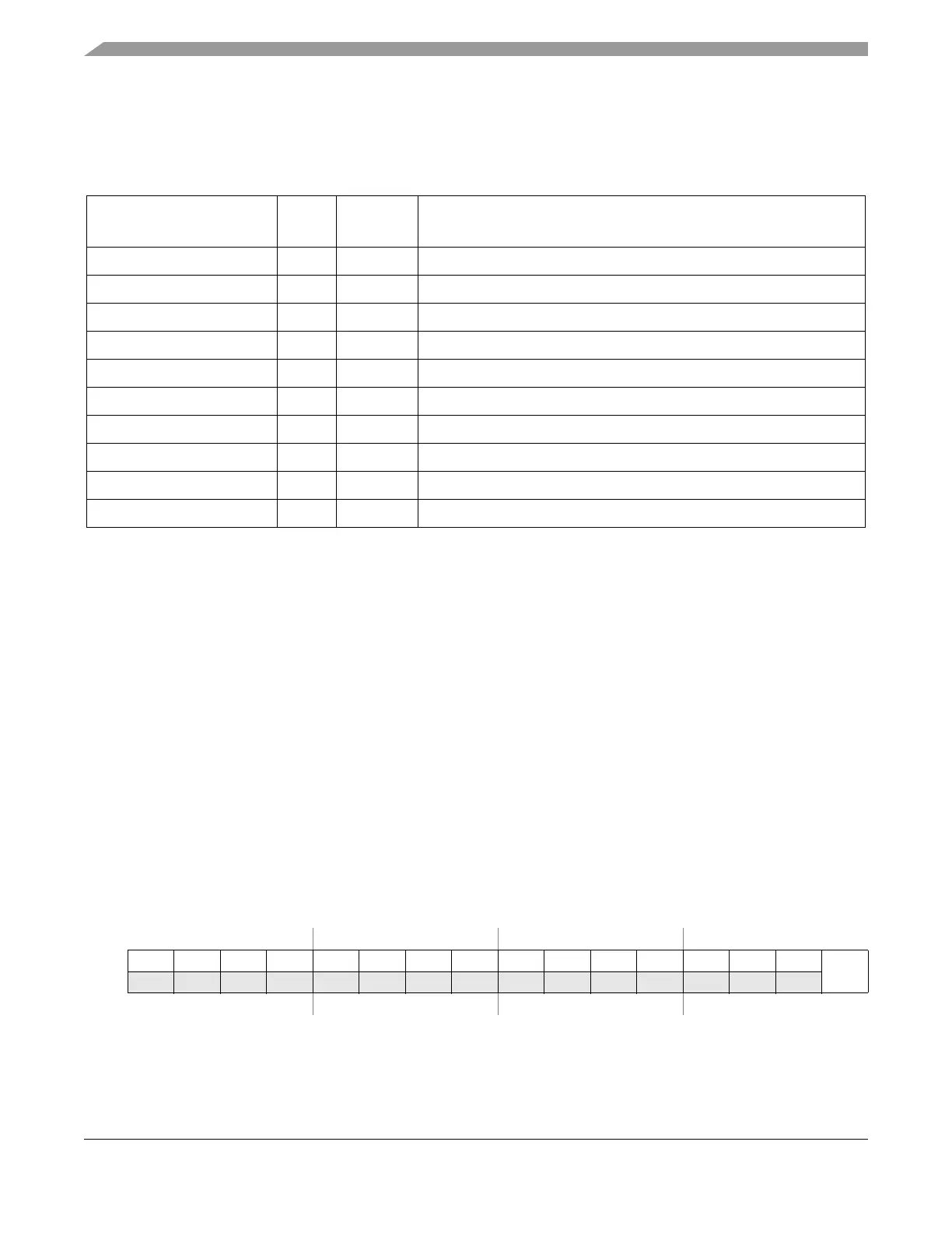
Table 6-1. MFR4310 Relevant Pins for the CRG
Pin Name
1
1
# – signal is active-low
In/Out
Pin
type
2,3,4
2
Acronyms:
PC – (Pullup/pulldown Controlled) Register controlled internal weak pullup/pulldown for a pin in the input mode
PU/PD – (Pullup/Pulldown) Internal weak pullup/pulldown for a pin in the input mode
DC – (Drive strength Controlled) Register controlled drive strength for a pin in the output mode
OD – (Open Drain) Output pin with open drain
Z – Tristated pin
3
No load allowed except for bypass capacitors.
4
Reset state: All pins with the PC option – pullup/pulldown is disabled,
All pins with the DC option – have full drive strength
Functional Description
TXD_BG2/IF_SEL0 I/O DC/PU PHY Data transmitter output / Host interface select
TXD_BG1/IF_SEL1 I/O DC/PD PHY Data transmitter output / Host interface select
CHICLK_CC I - External CHI clock input – selectable
CLKOUT I/O DC Controller clock output–selectable from: disabled, 4/10/40 MHz
RESET# I PD Hardware reset input
INT_CC# O OD/DC Controller interrupt output
TEST I PD Factory Test mode select– should be tied to logic low in application
DBG[3:2]/CLK_S[1:0] I/O DC/PD Debug strobe point / Output clock select
EXTAL/CLK_CC I - Crystal driver / External clock pin
XTAL I - Crystal driver pin
Address in MFR4310 = 0x00E0 Write: Any Time
1514131211109876543210
R000000000000000
CMIE
W
Reset0000000000000000
Figure 6-1. Detection Enable Register (DER)