Device Overview
MFR4310 Reference Manual, Rev. 2
52 Freescale Semiconductor
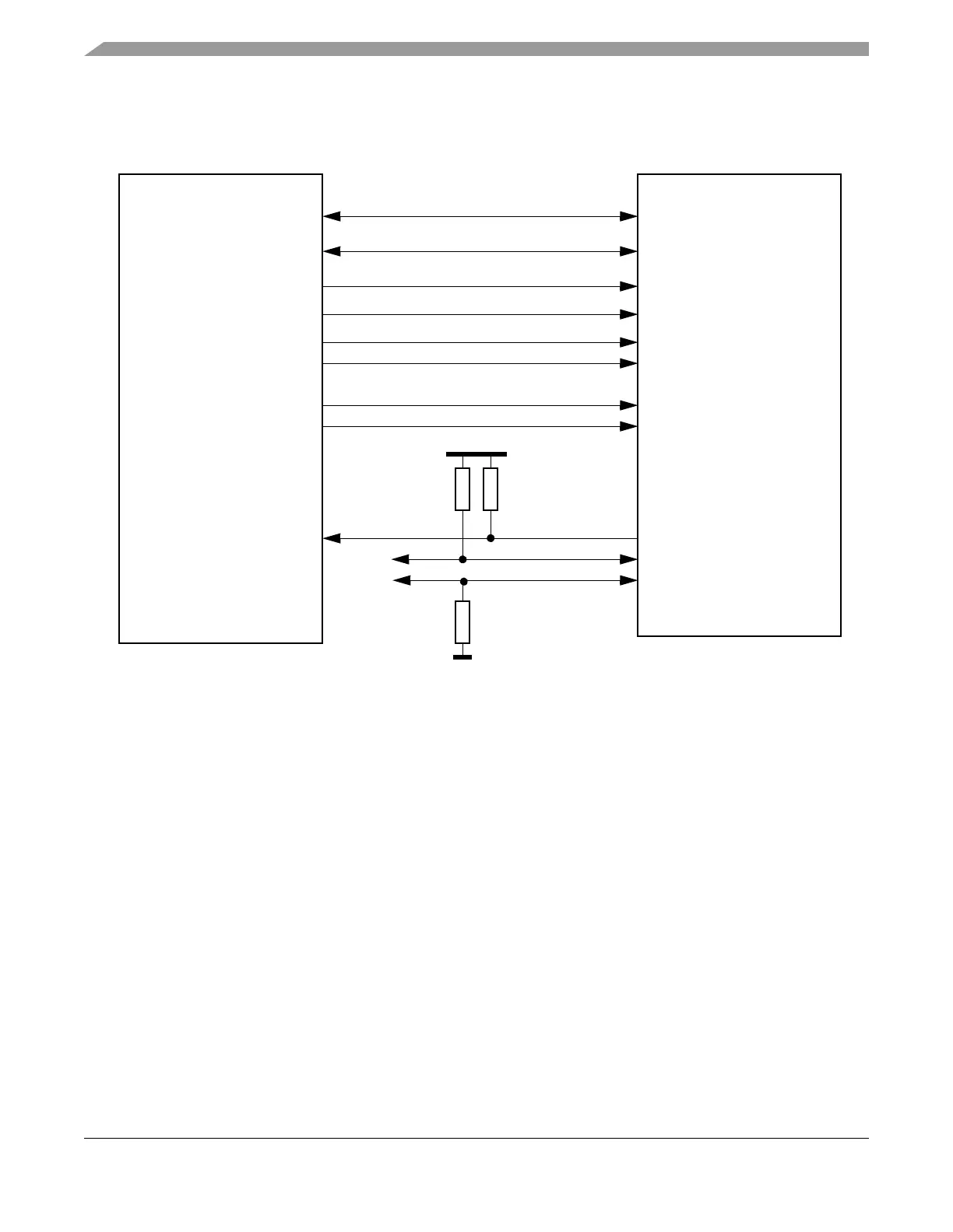
2.7.2.1 MPC Interface with MPC5xx and MPC55xx Families
Figure 2-7. MPC EBI Interface with MPC5xx and MPC55xx Families
2.7.2.2 MPC Interface Timing
See Section A.5, “MPC Interface Timing” for timing characteristics of the MPC interface.
2.7.3 HCS12 Interface
Chip selection for the HCS12 interface is generated internally using the following signals (see Figure 2-8):
• The input values of the expanded address signals XADDR[14:19] are compared with logical 0’s
(the HCS12 External Bus Interface (EBI) is in the Paged or Unpaged mode).
• The three most significant bits of the demultiplexed address bus, PA[5:7], are compared with the
pattern set up externally on the address chip select pins ACS[0:2]; PA5 is compared with ACS0,
PA6 with ACS1, PA7 with ACS2.
NOTE
The address decoding phase of a read/write operation is passed if all the
comparisons described above are passed.
MFR4310
MPC5xx Family
D0
DATA0 D15
DATA15
A1
ADDR19 A12
ADDR30
…
…
…
…
CE#
OE#
CSn#
OE#
INT_CC#
TXD_BG2/IF_SEL0
TXD_BG1/IF_SEL1
IRQn#
VDDXn
VSSXn
PL Interface
WE0/BE0
WE1/BE1
BSEL1#
BSEL0#
MPC55xx Family