Electrical Characteristics
MFR4310 Reference Manual, Rev. 2
252 Freescale Semiconductor
A.5 MPC Interface Timing
The CC MPC Interface read/write timing diagram is shown in the following figures.
• Writing to the device is accomplished when Chip Enable (CE#) and at least one of the Byte Selects
(BSEL[1:0]#) inputs are LOW (asserted).
• Reading from the device is accomplished when Chip Enable (CE#) and Output Enable (OE#) is
LOW (asserted) while both Byte Selects (BSEL[1:0]#) are HIGH (deasserted).
• The input/output pins (D[15:0]) are in a high-impedance state when the device is not selected (CE#
is HIGH), the outputs are disabled (OE# HIGH) or during a write operation (CE# LOW and at least
one BSEL[1:0]# LOW).
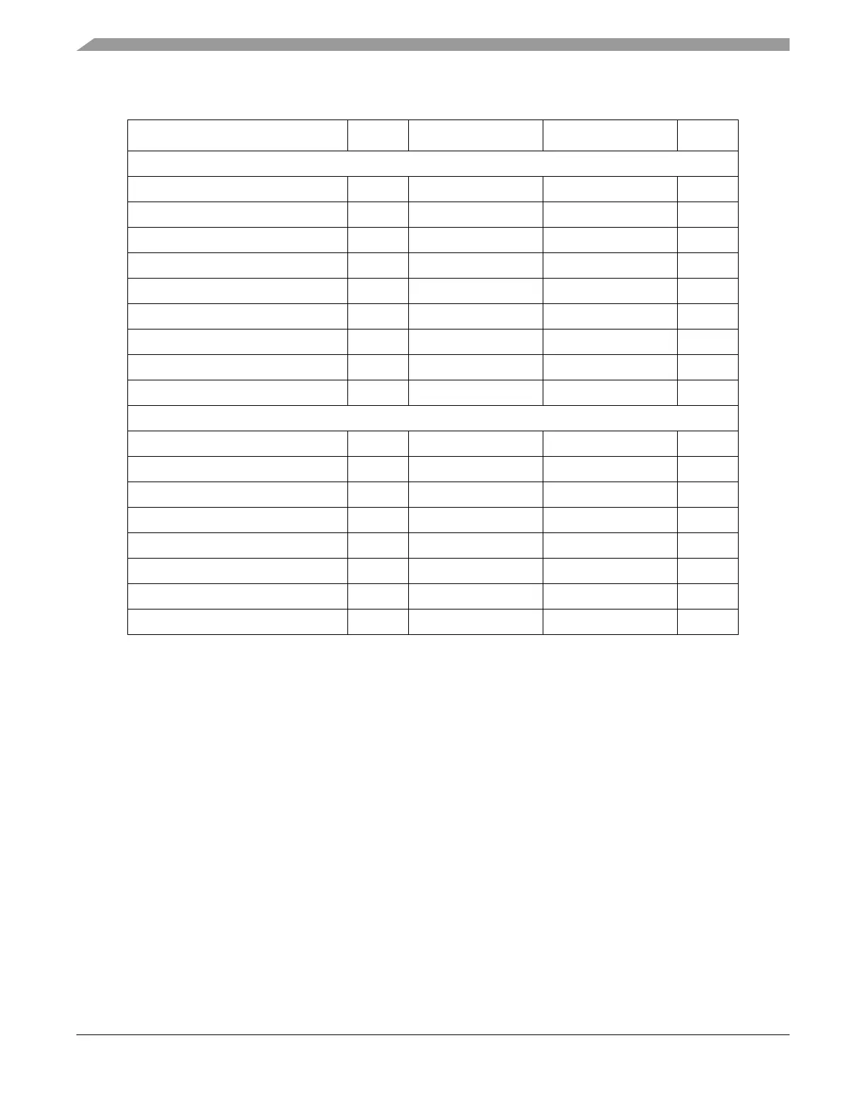
Table A-13. AMI Interface AC Switching Characteristics Over the Operating Range
1
1
t
AMI_CLK
is the period in ns of the CHI and host interface clock selected by IF_SEL[1:0] as described in
Table 2-6 .
Characteristic Symbol Min Max Unit
Read Cycle
Read Time Cycle t
RC
2.5 × t
AMI_CLK
+ 32 ns
Address Setup Read t
SAR
5ns
Address Hold Read t
HAR
5ns
OE# LOW to Data valid t
DOE
2.5 × t
AMI_CLK
+ 23 ns
OE# LOW time t
LOE
2.5 × t
AMI_CLK
+ 27
2
2
Depends on duty cycle of the CHI and host interface clock: t
LOE
= (3.0 × t
AMI_CLK
) - t
AMI_CLK_HIGH
+ 27,
where t
AMI_CLK_HIGH
is the period in ns of the high phase of the CHI and host interface clock.
ns
OE# HIGH time t
HOE
5ns
OE# LOW to Low-Z t
LZOE
5ns
OE# HIGH to High-Z t
HZOE
15 ns
WE# HIGH to OE# LOW t
WEOE
1 × t
AMI_CLK
ns
Write Cycle
Write Time Cycle t
WC
3 × t
AMI_CLK
+ 10 ns
Address Setup Write t
SAW
5ns
Address Hold Write t
HAW
5ns
Data Setup t
SD
5ns
Data Hold t
HD
5ns
WE# LOW time t
LWE
1.5 × t
AMI_CLK
+ 5 ns
WE# HIGH time t
HWE
0.5 × t
AMI_CLK
+ 5 ns
OE# HIGH to WE# LOW t
OEWE
0ns