Electrical Characteristics
MFR4310 Reference Manual, Rev. 2
Freescale Semiconductor 241
A.1.7 Operating Conditions
This section describes the operating conditions of the device. Unless otherwise noted those conditions
apply to all the following data.
NOTE
Refer to the temperature rating of the device (C, V, M) with regards to the
ambient temperature T
A
and the junction temperature T
J
. For power
dissipation calculations refer to Section A.1.8, “Power Dissipation and
Thermal Characteristics”.
A.1.8 Power Dissipation and Thermal Characteristics
Power dissipation and thermal characteristics are closely related. The user must assure that the maximum
operating junction temperature is not exceeded. The average chip-junction temperature (T
J
) in °C can be
obtained from:
Eqn. A-1
T
J
= Junction Temperature [°C]
T
A
= Ambient Temperature [°C]
P
D
= Total Chip Power Dissipation [W]
Θ
JA
= Package Thermal Resistance [°C/W]
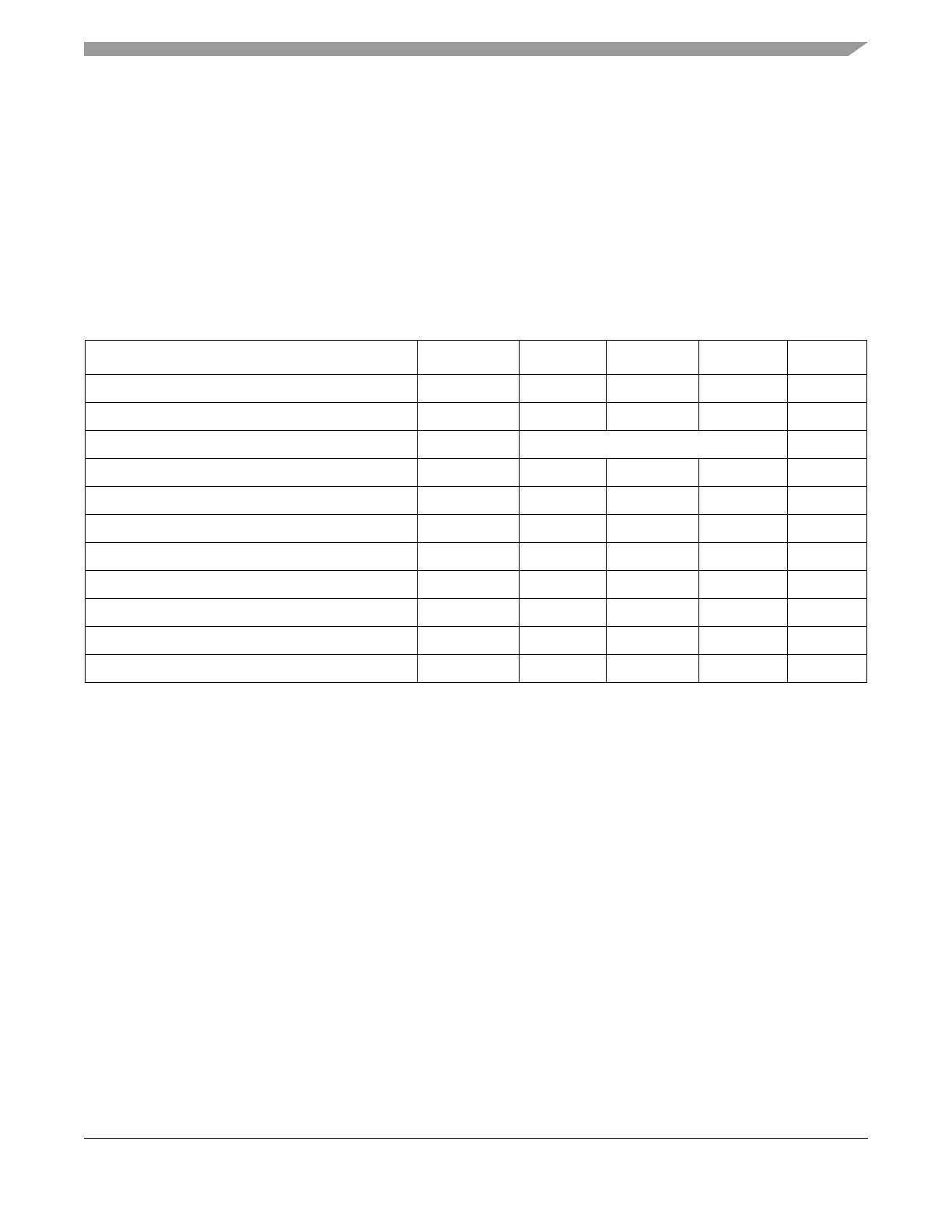
Table A-4. Operating Conditions
Rating Symbol Min Typ Max Unit
Oscillator and Quartz frequency
1
1
Input clock frequency applied to EXTAL/CLK_CC
f
OSC
- 40 40 MHz
Controller host interface clock frequency f
CHICLK_CC
20 - 76 MHz
Quartz overtone Fundamental Frequency
Quartz frequency stability at T
J
f
STB
-1500 300 1500 ppm
Voltage difference VDDX to VDDR and VDDA D
VDDX
-0.1 0 0.1 V
Voltage difference VSSX to VSSR and VSSA D
VSSX
-0.1 0 0.1 V
I/O, Regulator and Analog Supply V
DD5
2.97 3.3 5.5 V
Digital Logic Supply Voltage
2
2
The device contains an internal voltage regulator to generate the logic and OSC supply out of the I/O supply.
V
DD
2.25 2.5 2.75 V
Oscillator Supply Voltage
1
V
DDOSC
2.25 2.5 2.75 V
Operating Junction Temperature Range T
J
-40 - +140
o
C
Operating Ambient Temperature Range
3
3
Refer to Section A.1.8, “Power Dissipation and Thermal Characteristics” for more information about the relation between
ambient temperature T
A
and device junction temperature T
J
.
T
A
-40 +27 +125
o
C