Device Overview
MFR4310 Reference Manual, Rev. 2
Freescale Semiconductor 37
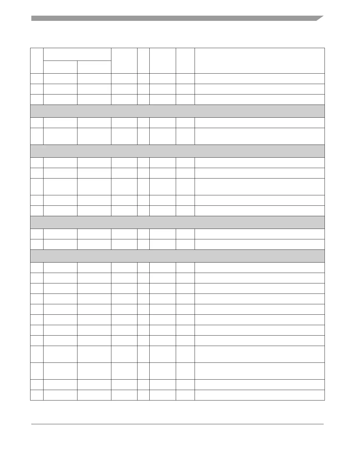
44 TXEN2# - VDDX O DC 1 Transmit enable for PHY
45 TXD_BG2 IF_SEL0 VDDX I/O DC/PU - PHY Data transmitter output / Host interface select
41 TXD_BG1 IF_SEL1 VDDX I/O DC/PD - PHY Data transmitter output / Host interface select
Clock Signals
32 CHICLK_CC - VDDX I - - External CHI clock input – selectable
63 CLKOUT - VDDX I/O DC - Controller clock output – selectable as disabled/4/10/40
MHz
Others
16 RESET# - VDDX I PD - External hardware reset input
64 INT_CC# - VDDX O OD/DC 0 Controller level-sensitive interrupt output
1 TEST - VDDX I PD - Factory Test mode select – must be tied to logic low in
application
42 DBG2 CLK_S0 VDDX I/O DC/PD - Debug strobe point / Output clock select
46 DBG3 CLK_S1 VDDX I/O DC/PD - Debug strobe point / Output clock select
Oscillator
24 EXTAL CLK_CC VDDOSC I - - Crystal driver / External clock
25 XTAL - - I - - Crystal driver
Supply/Bypass Filter pins
8 VDDX1 - - - - - Supply voltage, I/O
37 VDDX2 - - - - - Supply voltage, I/O
54 VDDX3 - - - - - Supply voltage, I/O
35 VDDX4 - - - - - Supply voltage, I/O
9 VSSX1 - - - - - Supply voltage ground, I/O
38 VSSX2 - - - - - Supply voltage ground, I/O
53 VSSX3 - - - - - Supply voltage ground, I/O
31 VSSX4 - - - - - Supply voltage ground, I/O
20 VDDR - - - - - Supply voltage, supply to pin drivers and internal
Voltage Regulator
19 VSSR - - - - - Supply voltage ground, ground to pin drivers and
internal Voltage Regulator
50 VDDA - - - - - Supply analog voltage
49 VSSA - - - - - Supply analog voltage ground
Table 2-3. Pin Functions and Signal Properties (continued)
Pin
#
Pin Name
1
Powered
by
I/O
Pin
Type
2, 3
Reset Functional Description
Function 1 Function 2