Overview
2.4.1.6 Dual Channel Resolver-to-Digital Converter PCB Assembly
(Optional POL and 4TH AXIS)
The Resolver-to-Digital Converter (RDC) PCB accepts analog inputs from the
antenna-mounted resolvers (via the rear panel termination circuit card) and provides
a binary digital encoded representation of the pointing angles for the POL and 4TH
AXIS to the CPU. VME bus interface circuitry is included, based upon CPU and
RDC timing requirements. The standard configuration is for single-speed resolvers
and 16-bit encoding.
2.4.1.7 IEEE-488 Interface (Optional)
The IEEE-488 bus has been optionally incorporated into the 7200 ACU to
accommodate users wishing to utilize this type of interface. The IEEE-488 bus
allows connectivity between different programmable devices with a standard
interface for communications between each instrument. The IEEE-488 interface is
also known as GPIB (General Purpose Interface Bus) or HPIB (Hewlett Packard
Interface Bus), and is electrically similar to IEC-625. Please refer to document CG-
6041 for M&C protocol for this interface.
2.4.1.8 Time and Frequency Processor Board (Optional)
The 7200 ACU clock accuracy can be precisely maintained by utilizing the optional
Time and Frequency Processor Board. This VME board is used in conjunction with
an external (CFE) time source to synchronize the 7200 ACU clock to the accurate
time source. The external time source sends an IRIG-B compliant signal to the J3
BNC connector on the rear of the 7200 ACU. This signal is routed to the Time and
Frequency Processor Board (TFP). The VCPU board acquires only the year from
the on-board real-time clock while the rest of the time/date information is taken
directly from the TFP board. If the TFP board becomes disconnected from its
source, a message will be displayed on the ACU “External Timing Source Lost”.
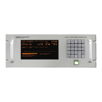
2.4.1.9 ACU Chassis Assembly
The ACU is housed in a custom chassis assembly which mounts in a standard 19-
inch Electronics Industry Association (EIA) rack, requiring 7-inches of vertical rack
space (4 Rack Units per EIA 310). The nominal overall dimensions of the ACU
chassis are: 7-inches tall by 19-inches wide by 20-inches deep. The 7200 ACU’s
weight is approximately 27 lbs. A four-slot VME card cage, which houses the
VCPU, I/O, and RDC PCB’s, is mounted to the inside of the chassis top plate. The
top plate is hinged at the rear of the chassis and includes a locking support arm to
facilitate convenient front-side access to the card cage. Studs connected to the
front panel support the front panel display and keypad and their respective control
circuit cards.
2-15