DocID13902 Rev 15 1072/1128
RM0008 Debug support (DBG)
1100
31.4.1 SWJ debug port pins
Five pins are used as outputs from the STM32F10xxx for the SWJ-DP as alternate functions
of general-purpose I/Os. These pins are available on all packages.
31.4.2 Flexible SWJ-DP pin assignment
After RESET (SYSRESETn or PORESETn), all five pins used for the SWJ-DP are assigned
as dedicated pins immediately usable by the debugger host (note that the trace outputs are
not assigned except if explicitly programmed by the debugger host).
However, the STM32F10xxx MCU implements the AF remap and debug I/O configuration
register (AFIO_MAPR) register to disable some part or all of the SWJ-DP port and so
releases the associated pins for General Purpose IOs usage. This register is mapped on an
APB bridge connected to the Cortex
®
-M3 System Bus. Programming of this register is done
by the user software program and not the debugger host.
Three control bits allow the configuration of the SWJ-DP pin assignments. These bits are
reset by the System Reset.
• AFIO_MAPR (@ 0x40010004 in the STM32F10xxx MCU)
– READ: APB - No Wait State
– WRITE: APB - 1 Wait State if the write buffer of the AHB-APB bridge is full.
Bit 26:24= SWJ_CFG[2:0]
Set and cleared by software.
These bits are used to configure the number of pins assigned to the SWJ debug port.
The goal is to release as much as possible the number of pins to be used as General
Purpose IOs if using a small size for the debug port.
The default state after reset is “000” (whole pins assigned for a full JTAG-DP
connection). Only one of the 3 bits can be set (it is forbidden to set more than one bit).
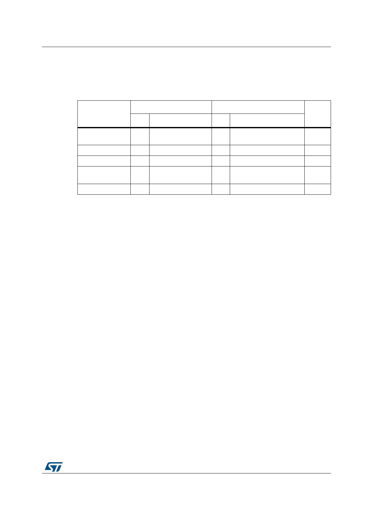
Table 218. SWJ debug port pins
SWJ-DP pin name
JTAG debug port SW debug port Pin
assign
ment
Type Description Type Debug assignment
JTMS/SWDIO I
JTAG Test Mode
Selection
IO
Serial Wire Data
Input/Output
PA13
JTCK/SWCLK I JTAG Test Clock I Serial Wire Clock PA14
JTDI I JTAG Test Data Input - - PA15
JTDO/TRACESWO O JTAG Test Data Output -
TRACESWO if async trace
is enabled
PB3
NJTRST I JTAG Test nReset - - PB4
 Loading...


