DocID13902 Rev 15 254/1128
RM0008 Digital-to-analog converter (DAC)
272
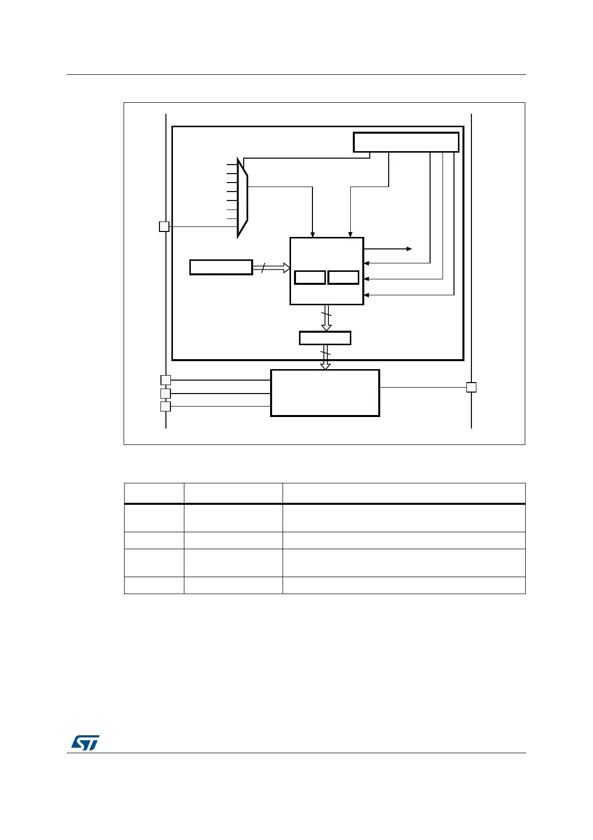
Figure 40. DAC channel block diagram
1. In connectivity line devices, the TIM8_TRGO trigger is replaced by TIM3_TRGO .
Note: Once the DAC channelx is enabled, the corresponding GPIO pin (PA4 or PA5) is
automatically connected to the analog converter output (DAC_OUTx). In order to avoid
parasitic consumption, the PA4 or PA5 pin should first be configured to analog (AIN).
Table 73. DAC pins
Name Signal type Remarks
V
REF+
Input, analog reference
positive
The higher/positive reference voltage for the DAC,
2.4 V
≤ V
REF
+ ≤ V
DDA
(3.3 V)
V
DDA
Input, analog supply Analog power supply
V
SSA
Input, analog supply
ground
Ground for analog power supply
DAC_OUTx Analog output signal DAC channelx analog output
V
DDA
V
SSA
V
REF+
DAC_ OU Tx
Control logicx
DHRx
12-bit
12-bit
LFSRx
trianglex
DM A reque stx
TSELx[2:0] bits
TIM4_T RGO
TIM5_T RGO
TIM6_T RGO
TIM7_T RGO
TIM2_T RGO
TIM8_TRGO
(1)
EXTI_9
DMAENx
TENx
MAMPx[3:0] bits
WAVENx[1:0] bits
SWTR IGx
DORx
Digital-to-analog
converterx
12-bit
DAC control register
ai14708c
Trigger selectorx
 Loading...


