DocID13902 Rev 15 250/1128
RM0008 Analog-to-digital converter (ADC)
252
11.12.13 ADC injected data register x (ADC_JDRx) (x= 1..4)
Address offset: 0x3C - 0x48
Reset value: 0x0000 0000
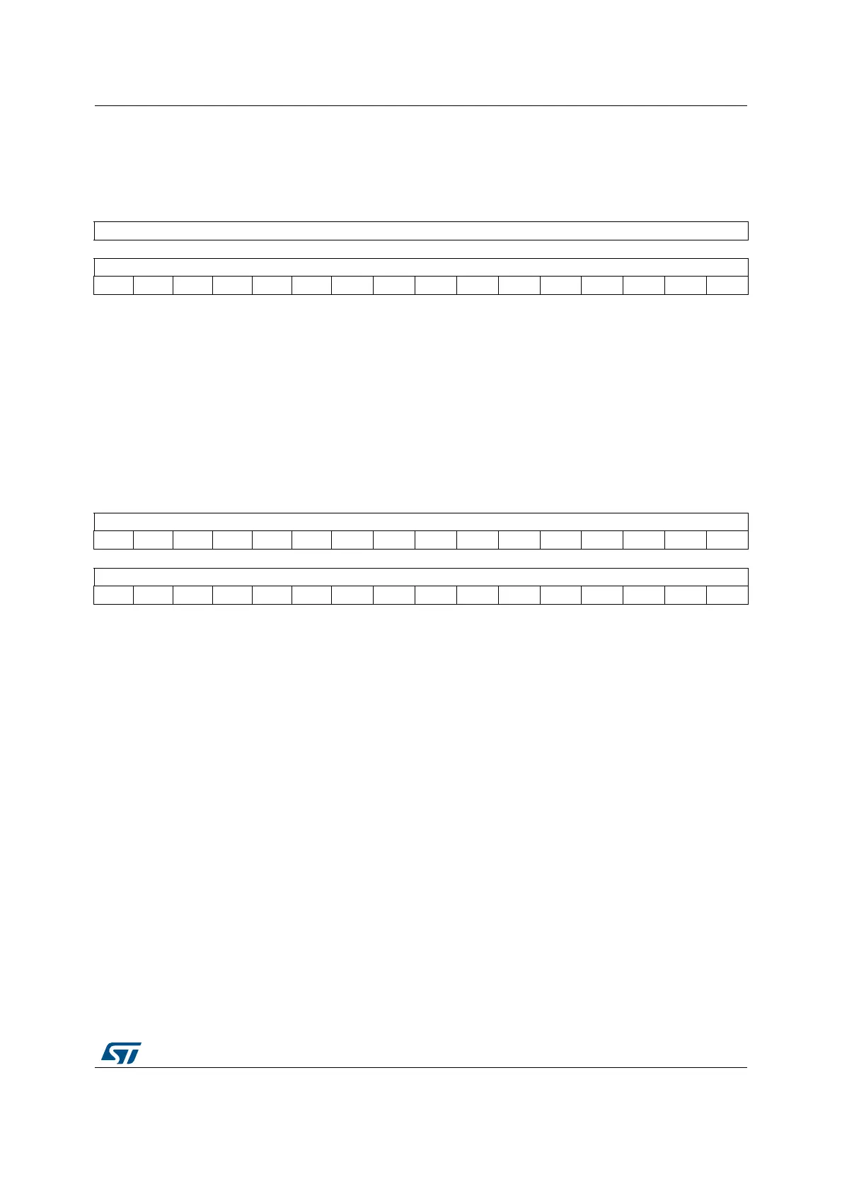
11.12.14 ADC regular data register (ADC_DR)
Address offset: 0x4C
Reset value: 0x0000 0000
31 30 29 28 27 26 25 24 23 22 21 20 19 18 17 16
Reserved
1514131211109876543210
JDATA[15:0]
rrrrrr r r r r rrrrrr
Bits 31:16 Reserved, must be kept at reset value.
Bits 15:0 JDATA[15:0]: Injected data
These bits are read only. They contain the conversion result from injected channel x. The
data is left or right-aligned as shown in Figure 27 and Figure 28.
31 30 29 28 27 26 25 24 23 22 21 20 19 18 17 16
ADC2DATA[15:0]
rrrrrr r r r r rrrrrr
1514131211109876543210
DATA[15:0]
rrrrrr r r r r rrrrrr
Bits 31:16 ADC2DATA[15:0]: ADC2 data
In ADC1: In dual mode, these bits contain the regular data of ADC2. Refer to Section 11.9:
Dual ADC mode.
In ADC2 and ADC3: these bits are not used.
Bits 15:0 DATA[15:0]: Regular data
These bits are read only. They contain the conversion result from the regular channels. The
data is left or right-aligned as shown in Figure 27 and Figure 28.
 Loading...


