Memory and bus architecture RM0008
61/1128 DocID13902 Rev 15
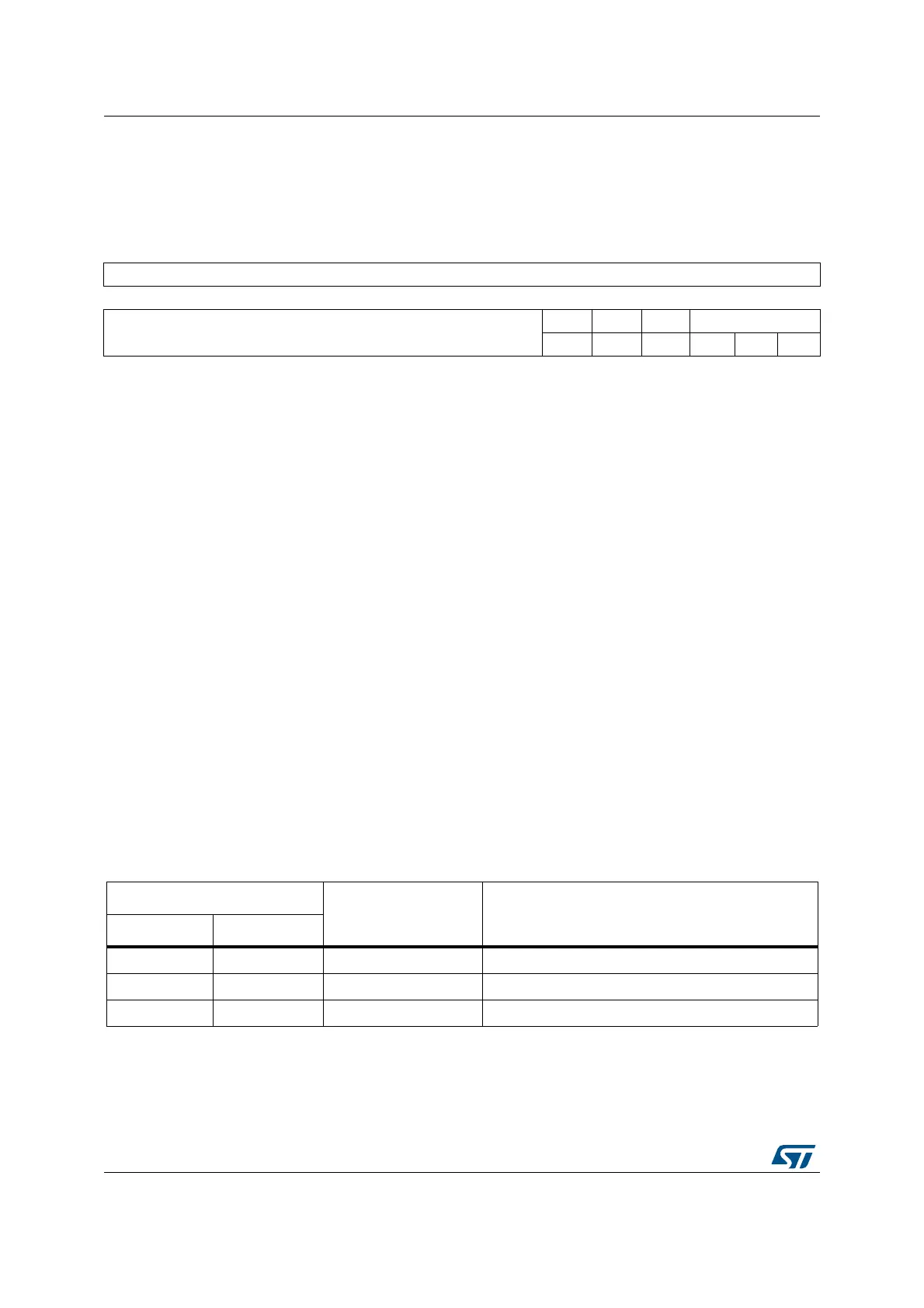
Flash access control register (FLASH_ACR)
Address offset: 0x00
Reset value: 0x0000 0030
3.4 Boot configuration
In the STM32F10xxx, 3 different boot modes can be selected through BOOT[1:0] pins as
shown in Table 9.
31 30 29 28 27 26 25 24 23 22 21 20 19 18 17 16
Reserved
15 14 13 12 11 10 9 8 7 6 5 4 3 2 1 0
Reserved
PRFTBS PRFTBE HLFCYA LATENCY
rrwrwrwrwrw
Bits 31:6 Reserved, must be kept at reset value.
Bit 5 PRFTBS: Prefetch buffer status
This bit provides the status of the prefetch buffer.
0: Prefetch buffer is disabled
1: Prefetch buffer is enabled
Bit 4 PRFTBE: Prefetch buffer enable
0: Prefetch is disabled
1: Prefetch is enabled
Bit 3 HLFCYA: Flash half cycle access enable
0: Half cycle is disabled
1: Half cycle is enabled
Bits 2:0 LATENCY: Latency
These bits represent the ratio of the SYSCLK (system clock) period to the Flash access
time.
000 Zero wait state, if 0 < SYSCLK≤ 24 MHz
001 One wait state, if 24 MHz < SYSCLK ≤ 48 MHz
010 Two wait states, if 48 MHz < SYSCLK ≤ 72 MHz
Table 9. Boot modes
Boot mode selection pins
Boot mode Aliasing
BOOT1 BOOT0
x 0 Main Flash memory Main Flash memory is selected as boot space
0 1 System memory System memory is selected as boot space
1 1 Embedded SRAM Embedded SRAM is selected as boot space
 Loading...


