General-purpose and alternate-function I/Os (GPIOs and AFIOs) RM0008
163/1128 DocID13902 Rev 15
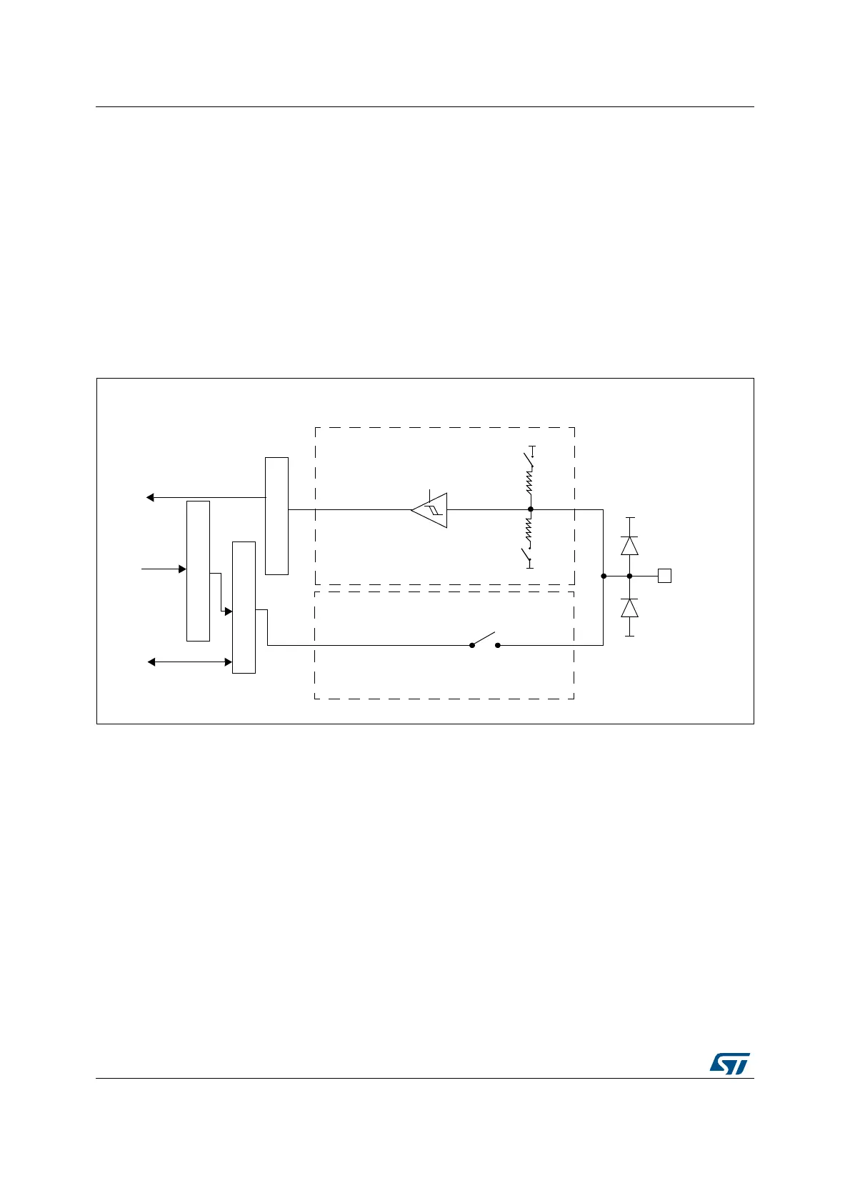
9.1.7 Input configuration
When the I/O Port is programmed as Input:
• The Output Buffer is disabled
• The Schmitt Trigger Input is activated
• The weak pull-up and pull-down resistors are activated or not depending on input
configuration (pull-up, pull-down or floating):
• The data present on the I/O pin is sampled into the Input Data Register every APB2
clock cycle
• A read access to the Input Data Register obtains the I/O State.
The Figure 15 on page 163 shows the Input Configuration of the I/O Port bit.
Figure 15. Input floating/pull up/pull down configurations
1. V
DD_FT
is a potential specific to five-volt tolerant I/Os and different from V
DD
.
I/O pin
TTL Schmitt
trigger
V
SS
V
DD
or V
DD_FT
(1)
protection
diode
protection
diode
on
input driver
output driver
Input data register
Output data register
Read/write
Read
Bit set/reset registers
Write
on/off
on/off
V
DD
V
SS
ai14783
 Loading...


