Ethernet (ETH): media access control (MAC) with DMA controller RM0008
965/1128 DocID13902 Rev 15
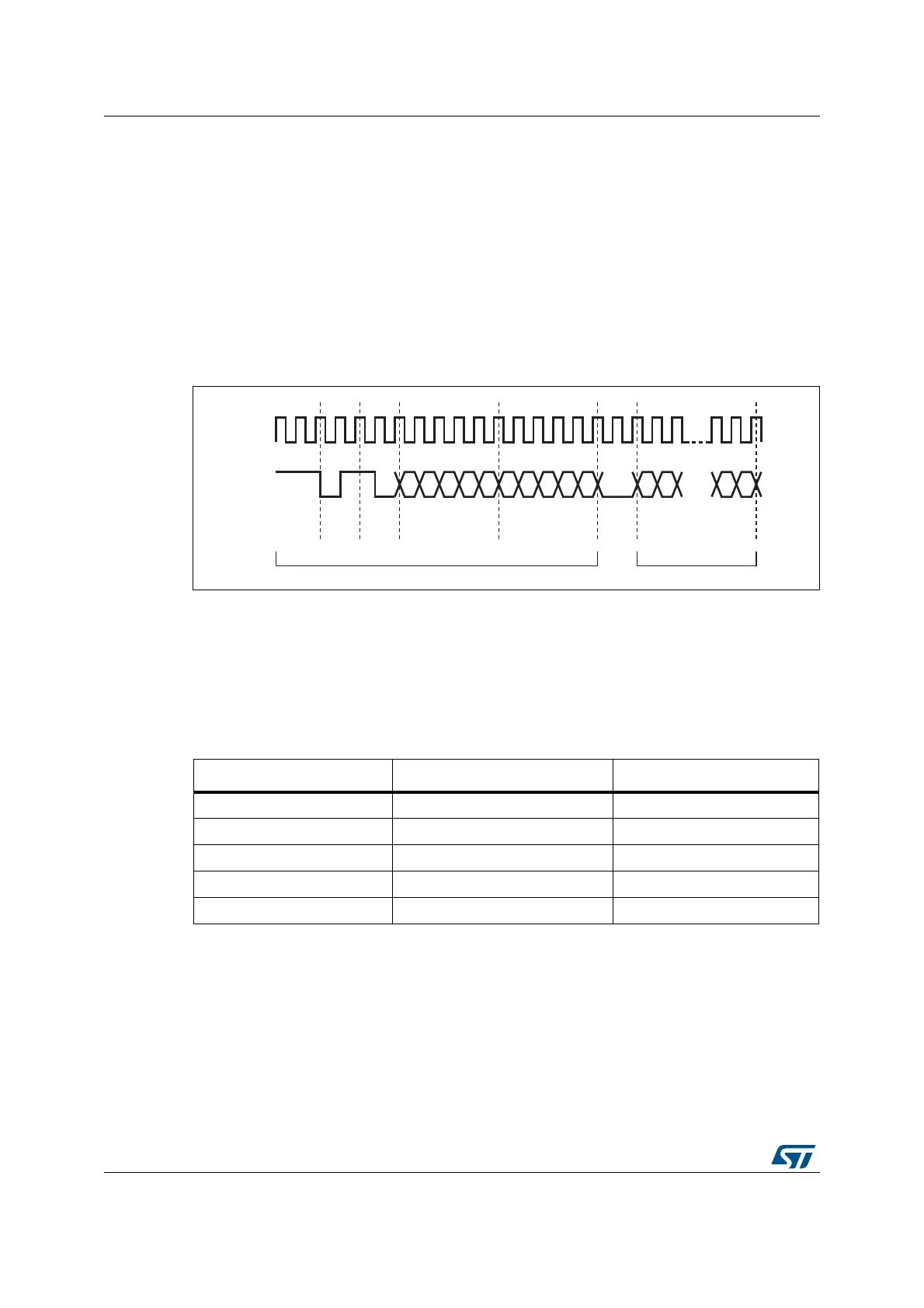
SMI read operation
When the user sets the MII Busy bit in the Ethernet MAC MII address register
(ETH_MACMIIAR) with the MII Write bit at 0, the SMI initiates a read operation in the PHY
registers by transferring the PHY address and the register address in PHY. The application
should not change the MII Address register contents or the MII Data register while the
transaction is ongoing. Write operations to the MII Address register or MII Data Register
during this period are ignored (the Busy bit is high) and the transaction is completed without
any error. After the read operation has completed, the SMI resets the Busy bit and then
updates the MII Data register with the data read from the PHY.
Figure 329 shows the frame format for the read operation.
Figure 329. MDIO timing and frame structure - Read cycle
SMI clock selection
The MAC initiates the Management Write/Read operation. The SMI clock is a divided clock
whose source is the application clock (AHB clock). The divide factor depends on the clock
range setting in the MII Address register.
Table 210 shows how to set the clock ranges.
Table 210. Clock range
Selection HCLK clock MDC clock
0000 60-72 MHz AHB clock / 42
0001 Reserved -
0010 20-35 MHz AHB clock / 16
0011 35-60 MHz AHB clock / 26
0100, 0101, 0110, 0111 Reserved -
MDC
MDIO
32 1's 0 1 1 0
A4 A3 A2 A1 A0 R4 R3 R2 R1 R0
D15 D14
D1 D0
Preamble
Start
of
frame
OP
code
PHY address Register address
Turn
around
data
Data to PHY
ai15627
Data from PHY
 Loading...


