Low-, medium-, high- and XL-density reset and clock control (RCC) RM0008
115/1128 DocID13902 Rev 15
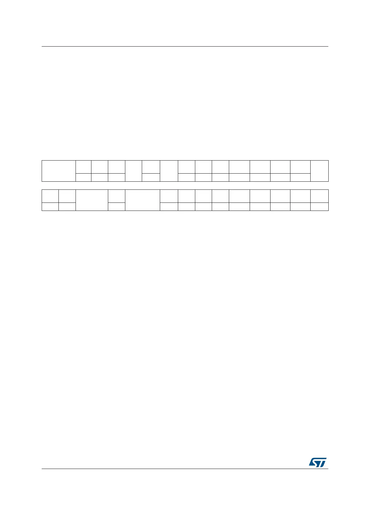
7.3.8 APB1 peripheral clock enable register (RCC_APB1ENR)
Address: 0x1C
Reset value: 0x0000 0000
Access: word, half-word and byte access
No wait state, except if the access occurs while an access to a peripheral on APB1 domain
is on going. In this case, wait states are inserted until this access to APB1 peripheral is
finished.
Note: When the peripheral clock is not active, the peripheral register values may not be readable
by software and the returned value is always 0x0.
31 30 29 28 27 26 25 24 23 22 21 20 19 18 17 16
Reserved
DAC
EN
PWR
EN
BKP
EN
Res.
CAN
EN
Res.
USB
EN
I2C2
EN
I2C1
EN
UART5E
N
UART4E
N
USART3
EN
USART2
EN
Res.
rw rw rw rw rw rw rw rw rw rw rw
15 14 13 12 11 10 9 8 7 6 5 4 3 2 1 0
SPI3
EN
SPI2
EN
Reserved
WWD
GEN
Reserved
TIM14
EN
TIM13
EN
TIM12
EN
TIM7
EN
TIM6
EN
TIM5
EN
TIM4
EN
TIM3
EN
TIM2
EN
rw rw rw rw rw rw rw rw rw rw rw rw
Bits 31:30 Reserved, must be kept at reset value.
Bit 29 DACEN: DAC interface clock enable
Set and cleared by software.
0: DAC interface clock disabled
1: DAC interface clock enable
Bit 28 PWREN: Power interface clock enable
Set and cleared by software.
0: Power interface clock disabled
1: Power interface clock enable
Bit 27 BKPEN: Backup interface clock enable
Set and cleared by software.
0: Backup interface clock disabled
1: Backup interface clock enabled
Bit 26 Reserved, must be kept at reset value.
Bit 25 CANEN: CAN clock enable
Set and cleared by software.
0: CAN clock disabled
1: CAN clock enabled
Bit 24 Reserved, always read as 0.
Bit 23 USBEN: USB clock enable
Set and cleared by software.
0: USB clock disabled
1: USB clock enabled
 Loading...


