Inter-integrated circuit (I
2
C) interface RM0008
757/1128 DocID13902 Rev 15
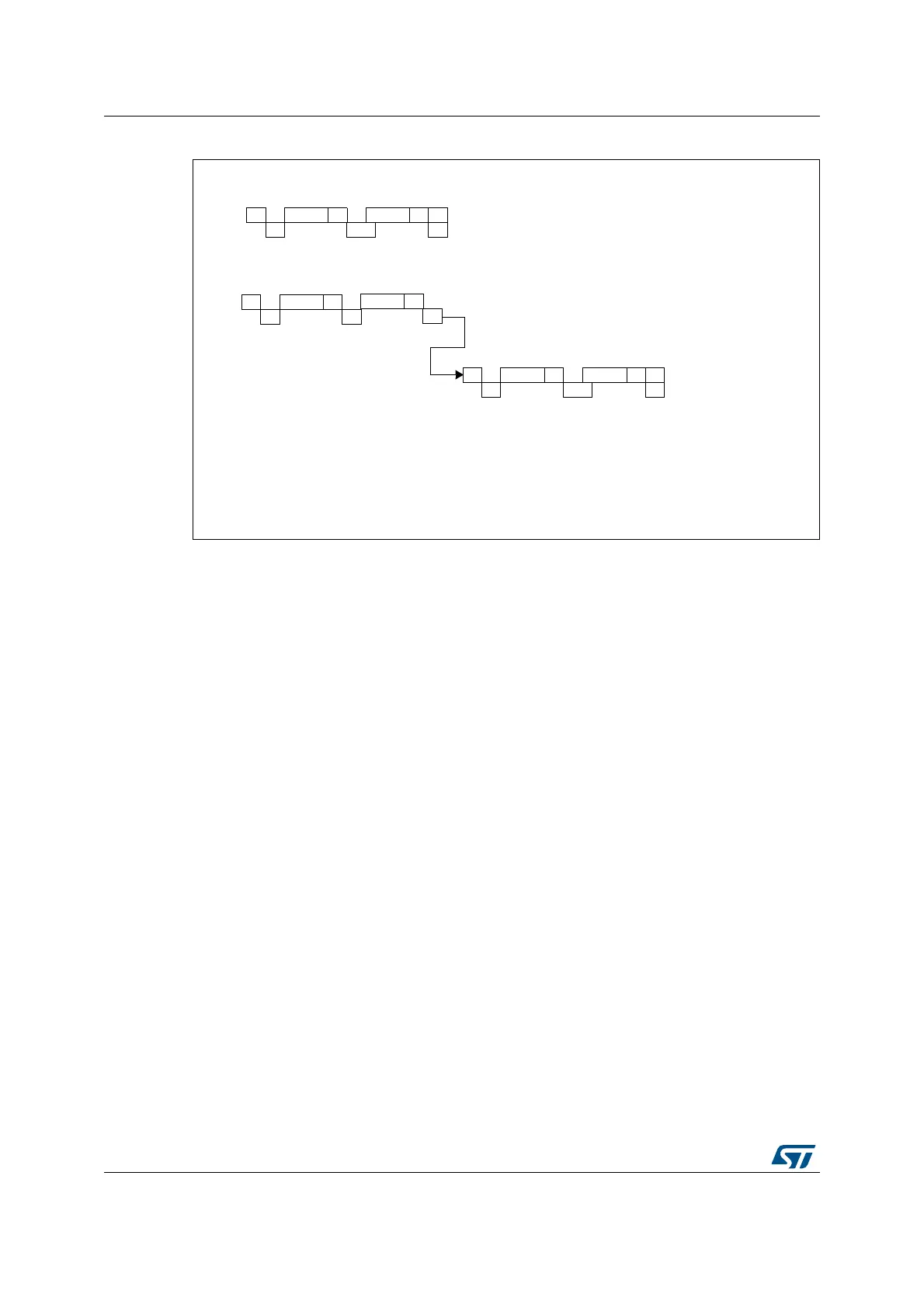
Figure 276. Method 2: transfer sequence diagram for master receiver when N=1
1. The EV5, EV6 and EV9 events stretch SCL low until the end of the corresponding software sequence.
26.3.4 Error conditions
The following are the error conditions which may cause communication to fail.
Bus error (BERR)
This error occurs when the I
2
C interface detects an external Stop or Start condition during
an address or a data transfer. In this case:
• the BERR bit is set and an interrupt is generated if the ITERREN bit is set
• in Slave mode: data are discarded and the lines are released by hardware:
– in case of a misplaced Start, the slave considers it is a restart and waits for an
address, or a Stop condition
– in case of a misplaced Stop, the slave behaves like for a Stop condition and the
lines are released by hardware
• In Master mode: the lines are not released and the state of the current transmission is
not affected. It is up to the software to abort or not the current transmission
Acknowledge failure (AF)
This error occurs when the interface detects a nonacknowledge bit. In this case:
• the AF bit is set and an interrupt is generated if the ITERREN bit is set
• a transmitter which receives a NACK must reset the communication:
– If Slave: lines are released by hardware
– If Master: a Stop or repeated Start condition must be generated by software
AAddressS
EV5
NAData1
EV7
P
Legend: S = Start, S
r
= Repeated Start, P = Stop, A = Acknowledge, NA = Non-acknowledge,
EV5: SB=1, cleared by reading SR1 register followed by writing the DR register.
EV6_3: ADDR = 1, program ACK = 0, clear ADDR by reading SR1 register followed by reading SR2 register, program
.
EV6_3
STOP =1 just after ADDR is cleared.
Note: The EV6_3 software sequence must complete before the current byte end of transfer.
10- bit master receiver
AHeaderS
EV5 EV9
AAddress
EV6
7- bit master receiver
NAData1
EV7
P
EV6_3
AHeaderS
r
EV5
EV9: ADD10= 1, cleared by reading SR1 register followed by writing DR register.
EVx = Event (with interrupt if ITEVFEN = 1)
EV7: RxNE =1, cleared by reading DR register.
EV6: ADDR =1, cleared by reading SR1 resister followed by reading SR2 register.
 Loading...


