Flexible static memory controller (FSMC) RM0008
543/1128 DocID13902 Rev 15
the NAND Flash device is active during the write strobe (low pulse on NWE), thus the
written bytes are interpreted as the start address for read operations. Using the
attribute memory space makes it possible to use a different timing configuration of the
FSMC, which can be used to implement the prewait functionality needed by some
NAND Flash memories (see details in Section 21.6.5: NAND Flash pre-wait
functionality on page 543).
4. The controller waits for the NAND Flash to be ready (R/NB signal high) to become
active, before starting a new access (to same or another memory bank). While waiting,
the controller maintains the NCE signal active (low).
5. The CPU can then perform byte read operations in the common memory space to read
the NAND Flash page (data field + Spare field) byte by byte.
6. The next NAND Flash page can be read without any CPU command or address write
operation, in three different ways:
– by simply performing the operation described in step 5
– a new random address can be accessed by restarting the operation at step 3
– a new command can be sent to the NAND Flash device by restarting at step 2
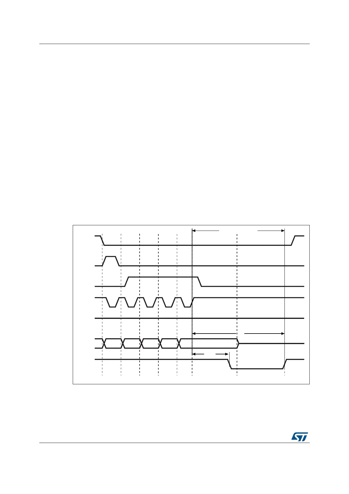
21.6.5 NAND Flash pre-wait functionality
Some NAND Flash devices require that, after writing the last part of the address, the
controller wait for the R/NB signal to go low as shown in Figure 205.
Figure 205. Access to non ‘CE don’t care’ NAND-Flash
1. CPU wrote byte 0x00 at address 0x7001 0000.
2. CPU wrote byte A7-A0 at address 0x7002 0000.
3. CPU wrote byte A15-A8 at address 0x7002 0000.
4. CPU wrote byte A23-A16 at address 0x7002 0000.
5. CPU wrote byte A25-A24 at address 0x7802 0000: FSMC performs a write access using FSMC_PATT2
.#%
./%
)/;=
2."
AIB
(IGH
T7"
#,%
!,%
X !! !! !! !!
T2
.7%
.#%MUSTSTAYLOW
 Loading...


