DocID13902 Rev 15 178/1128
RM0008 General-purpose and alternate-function I/Os (GPIOs and AFIOs)
195
9.3.7 Timer alternate function remapping
Timer 4 channels 1 to 4 can be remapped from Port B to Port D. Other timer remapping
possibilities are listed in Table 44 to Table 46. Refer to AF remap and debug I/O
configuration register (AFIO_MAPR).
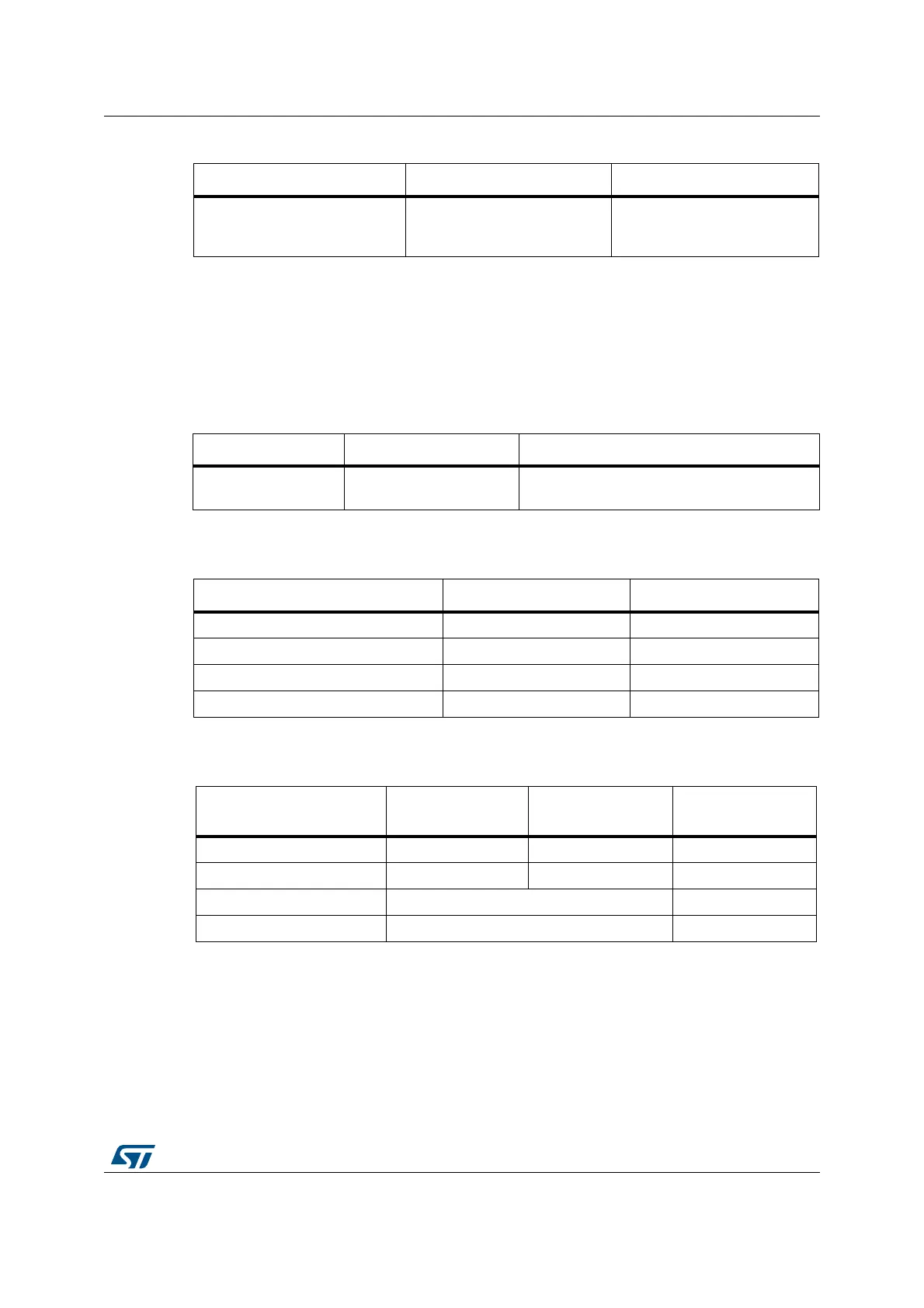
Table 41. ADC2 external trigger regular conversion alternate function remapping
(1)
1. Remap available only for high-density and XL-density devices.
Alternate function ADC2_ETRGREG_REG = 0 ADC2_ETRGREG_REG = 1
ADC2 external trigger regular
conversion
ADC2 external trigger regular
conversion is connected to
EXTI11
ADC2 external trigger regular
conversion is connected to
TIM8_TRGO
Table 42. TIM5 alternate function remapping
(1)
1. Remap available only for high-density, XL-density and connectivity line devices.
Alternate function TIM5CH4_IREMAP = 0 TIM5CH4_IREMAP = 1
TIM5_CH4
TIM5 Channel4 is
connected to PA3
LSI internal clock is connected to TIM5_CH4
input for calibration purpose.
Table 43. TIM4 alternate function remapping
Alternate function TIM4_REMAP = 0 TIM4_REMAP = 1
(1)
1. Remap available only for 100-pin and for 144-pin package.
TIM4_CH1 PB6 PD12
TIM4_CH2 PB7 PD13
TIM4_CH3 PB8 PD14
TIM4_CH4 PB9 PD15
Table 44. TIM3 alternate function remapping
Alternate function
TIM3_REMAP[1:0] =
“00” (no remap)
TIM3_REMAP[1:0] =
“10” (partial remap)
TIM3_REMAP[1:0] =
“11” (full remap)
(1)
1. Remap available only for 64-pin, 100-pin and 144-pin packages.
TIM3_CH1 PA6 PB4 PC6
TIM3_CH2 PA7 PB5 PC7
TIM3_CH3 PB0 PC8
TIM3_CH4 PB1 PC9
 Loading...


